Semiconductor integrated circuit device

a technology of integrated circuit and semiconductor, applied in semiconductor devices, semiconductor/solid-state device details, electrical apparatus, etc., can solve the problems of insufficient noise reduction effect, serious power supply noise, and serious countermeasures against esd for the decoupling capacitor itself, so as to improve the esd robustness of the capacitor. , the effect of large area

Inactive Publication Date: 2010-10-07
RENESAS ELECTRONICS CORP
View PDF12 Cites 8 Cited by
  • Summary
  • Abstract
  • Description
  • Claims
  • Application Information

AI Technical Summary

Benefits of technology

[0019]In one embodiment, a semiconductor integrated circuit device includes a power supply line connected to a power supply terminal, a ground line connected to a ground terminal and a plurality of capacitors connected in parallel between the power supply line and the ground line. The plurality of capacitors include a first capacitor arranged at a first distance from one of the terminals and a second capacitor arranged at a second distance which is larger than the first distance from the one of the terminals, and the first capacitor has a larger area than the second capacitor. By having a large-shaped capacitance device near external terminals where more current flows, it is possible to improve ESD robustness of the capacitor itself. Furthermore, mounting a plurality of capacitors in different shapes enables to correspond to noise of various frequencies.
[0020]The present invention is able to provide a semiconductor integrated circuit device having a decoupling capacitor capable of achieving both the noise countermeasure of a circuit and ESD protection.

Problems solved by technology

With increasing number of devices and higher speed of LSI (Large Scale Integration), the problem of power supply noise is becoming serious.
In recent years, the countermeasure against ESD for the decoupling capacitor itself is posing a serious problem due to a thinner gate insulating film.
A change in the circuit size and capacity to mount may cause insufficient noise reduction effect by the decoupling capacitor.
By increasing number of devices and higher speed of LSI, diversification of power supply noise and high frequency noise in each functional block inside a chip are becoming a problem.
However, as generated noises are different for each circuit, it cannot be supported by one resonant circuit and a filter circuit.
Moreover, Ogawa does not support the types of noises (frequency characteristics of a capacitor).
However, such consideration has not been made for the arrangement of conventional decoupling capacitors.
Furthermore, by a thinner insulating film of a decoupling capacitor (gate insulating film in case of a MOS capacitance), ESD robustness of the decoupling capacitor itself has become a problem.
However, both ESD robustness of a decoupling capacitor and noise reduction have not simultaneously been taken into consideration.

Method used


Image

  • Semiconductor integrated circuit device
  • Semiconductor integrated circuit device
  • Semiconductor integrated circuit device

Examples


first embodiment

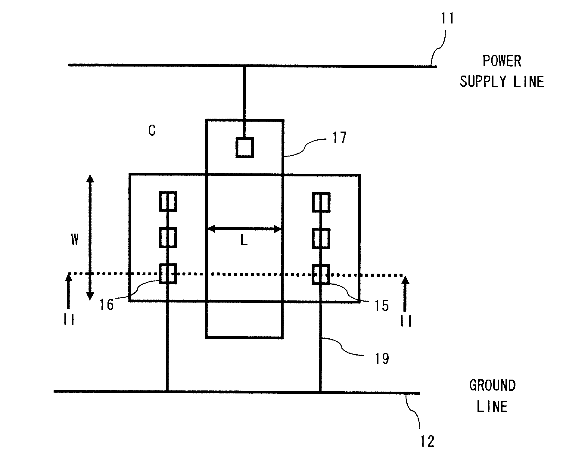
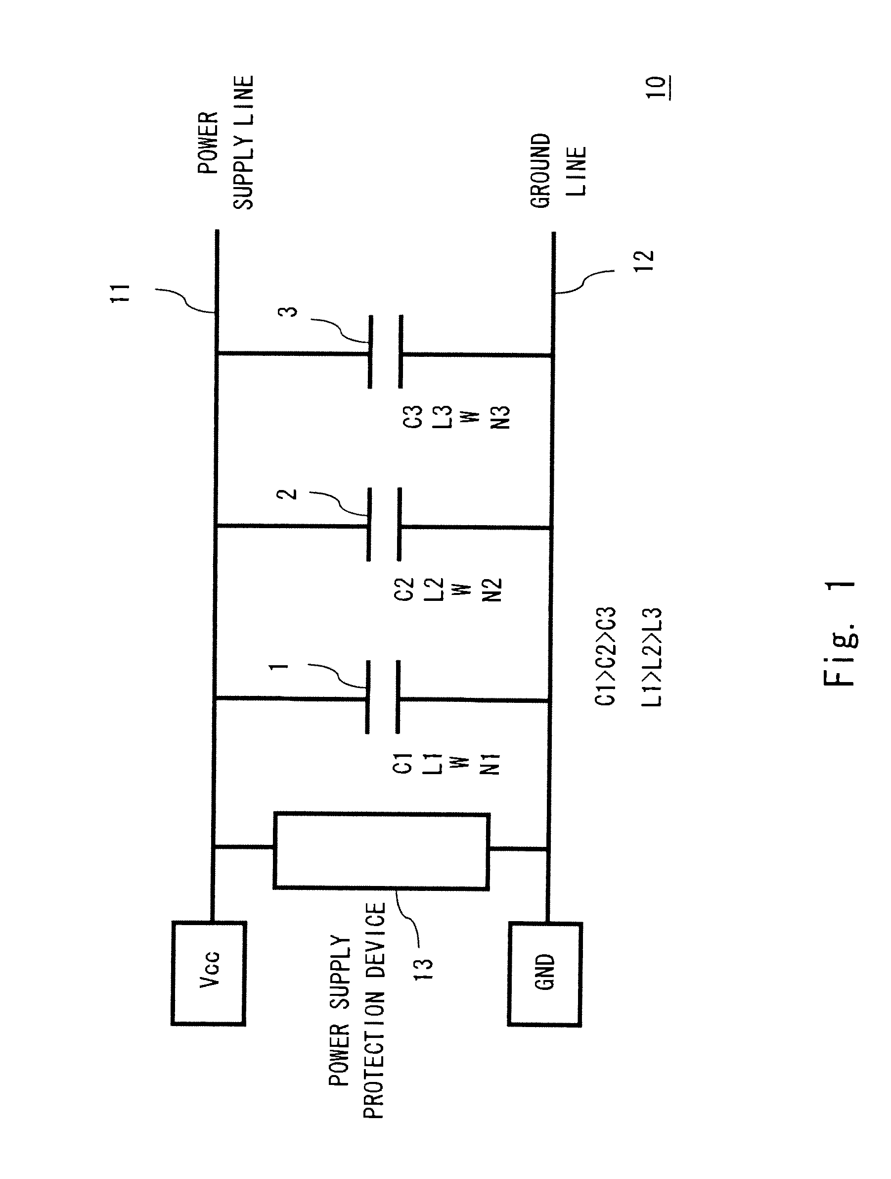
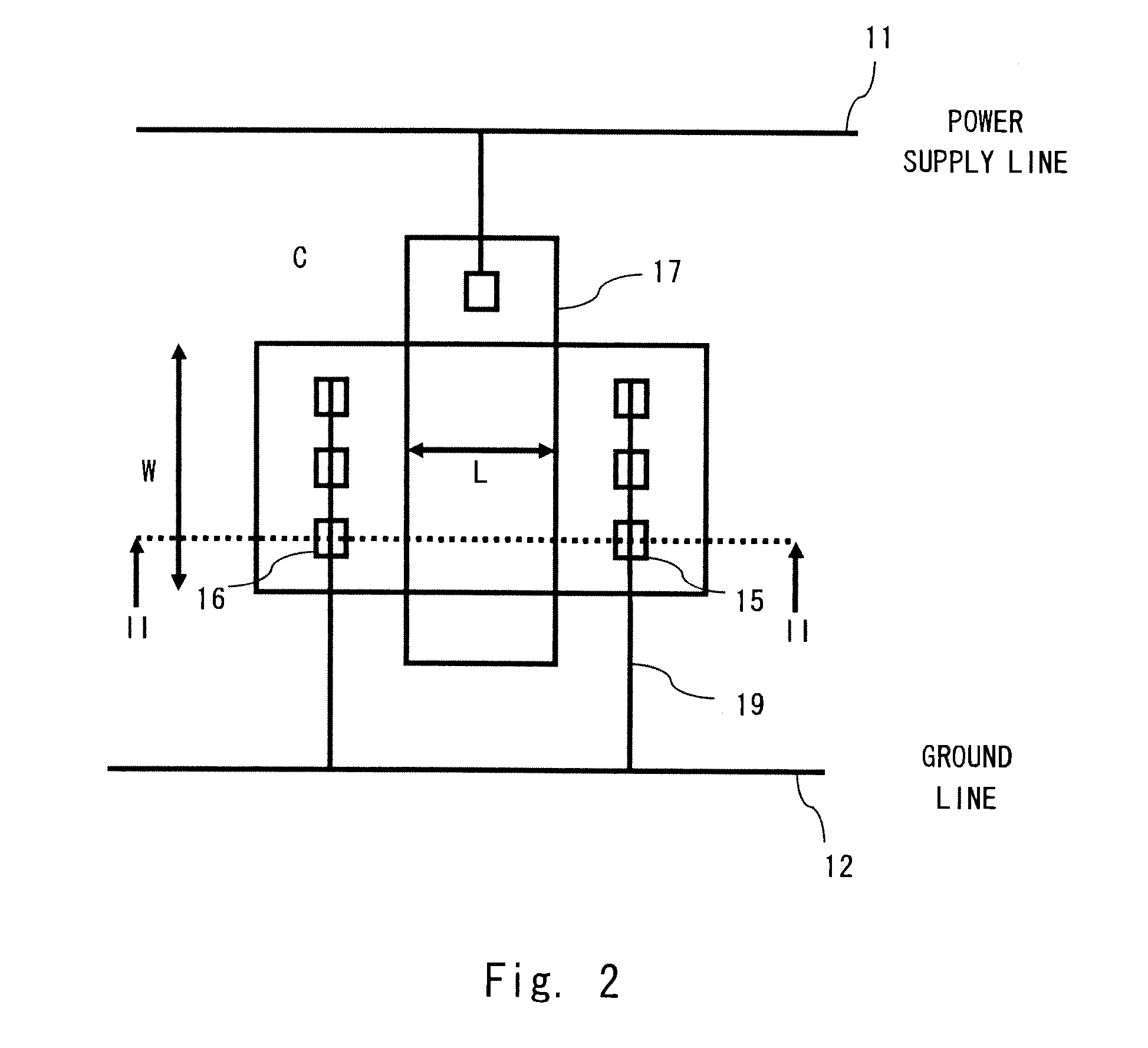
[0036]A first embodiment of the present invention is explained with reference to FIGS. 1 to 3. FIG. 1 shows the circuit configuration of a semiconductor integrated circuit device 10 according to this embodiment. Moreover, FIG. 2 is a plane view of a MOS capacitance device mounted to the semiconductor integrated circuit device 10 of this embodiment. FIG. 3 is a cross-sectional diagram taken along the line II-II of FIG. 2. Note that the internal circuit is omitted in FIG. 1.

[0037]As shown in FIG. 1, the semiconductor integrated circuit device 10 of this embodiment includes a power supply terminal Vcc, a ground terminal GND, a power supply line 11, a ground line 12, a power supply protection device 13 and capacitors 1, 2 and 3. In this embodiment, the capacitors 1, 2 and 3 are all formed of N type MOS capacitance devices. Note that in this embodiment, although the example of a semiconductor integrated circuit device having 3 capacitors is explained, it is not limited to this. Moreover,...

second embodiment

[0049]A semiconductor integrated circuit device 20 according to a second embodiment of the present invention is explained with reference to FIG. 4. FIG. 4 shows the configuration of the semiconductor integrated circuit device 20 according to this embodiment. There are many power supply lines and ground lines in the whole LSI. The power supply line and the ground line each have a trunk line and its branch line. As shown in FIG. 4, the semiconductor integrated circuit device 20 of this embodiment includes a power supply terminal Vcc, a ground terminal GND, a power supply line 21, a ground line 22 and a functional circuit block 29. The power supply line 21 includes a trunk line 23 and a branch line 25. Moreover, the ground line 22 includes a trunk line 24 and a branch line 26. The trunk line 23 is extended from the power supply terminal Vcc. Then, the branch line 25 is extended and branches from the trunk line 23. On the other hand, the trunk line 24 is extended from the ground termina...

third embodiment

[0056]A semiconductor integrated circuit device 30 according to a third embodiment of the present invention is explained with reference to FIG. 5. FIG. 5 shows the configuration of the semiconductor integrated circuit device 30 of this embodiment. A difference in this embodiment from the first embodiment shown in FIG. 1 is the locating position of the power supply terminal Vcc and the ground line GND.

[0057]As shown in FIG. 5, a power supply line 31 extended from the power supply terminal Vcc is formed toward the ground terminal GND side. Moreover, a ground line 32 extended from ground terminal GND is formed toward the power supply terminal Vcc side. Between the power supply line 31 and the ground line 32, a power supply protection device 33, capacitors 34, 35, and 36 and a power supply protection device 37 are provided from the ground terminal GND side to the power supply terminal Vcc side. That is, the distance from the power supply terminal Vcc to the capacitor 34 differs from the...


PUM


Abstract

A semiconductor integrated circuit device includes a power supply line connected to a power supply terminal, a ground line connected to a ground terminal and a plurality of capacitors connected in parallel between the power supply line and the ground line. The plurality of capacitors include a first capacitor arranged at a first distance from one of the terminals and a second capacitor arranged at a second distance which is larger than the first distance from the one of the terminals, and the first capacitor has a larger area than the second capacitor.

Description

[0001]CROSS-REFERENCE TO RELATED PATENT APPLICATIONS[0002]This application is a continuation of application Ser. No. 11 / 987,854, filed Dec. 5, 2007, now pending, and based on Japanese Patent Application No. 2006-331618, filed Dec. 8, 2006, by Hiroshi Furuta, which is incorporated herein by reference in its entirety. This application claims only subject matter disclosed in the parent application and therefore presents no new matter.BACKGROUND OF THE INVENTION[0003]1. Field of the Invention[0004]The present invention relates to a semiconductor integrated circuit device, and particularly to a semiconductor integrated circuit device having a decoupling capacitor (on chip capacitor).[0005]2. Description of Related Art[0006]With increasing number of devices and higher speed of LSI (Large Scale Integration), the problem of power supply noise is becoming serious. As a countermeasure against this power supply noise, the method of connecting a power source line and a ground line by a decoupli...

Claims


Application Information

Patent Timeline
Patent Type & Authority Applications(United States)
IPC IPC(8): H01L29/92
CPCH01L23/5223H01L23/5286H01L27/0248H01L2924/0002H01L2924/00
Inventor FURUTA, HIROSHI
Owner RENESAS ELECTRONICS CORP
Why Eureka
Try Eureka