Multi-Bit Resistance-Switching Memory Cell

Active Publication Date: 2010-10-07
SANDISK TECH LLC
View PDF34 Cites 10 Cited by
  • Summary
  • Abstract
  • Description
  • Claims
  • Application Information

AI Technical Summary

Benefits of technology

[0008]A storage system is described that uses reversible resistance-switching elements. Various circuits and methods are disclosed for controlling the reading, setting and resetting of the resistance for the reversible resistance-switching elements.
[0009]One embodiment of a non-volatile storage apparatus comprises a set of Y lines, a set of X lines and a plurality of memory cells in communication with the set of X lines and the set of Y lines. Each memory cell of the plurality of memory cells includes a resistance element in a static resistance condition and two or more reversible resistance-switching elements. The resistance element in the static resistance condition and the two or more reversible resistance-switching elements are connected to different Y lines of the set of Y lines. The resistance element in the static resistance condition and the two or more reversible resistance-switching elements are connected to a common X line of the set of X lines.
[0010]One embodiment of a non-volatile storage apparatus comprises an X line; a first Y line; a second Y line; a third Y line; a semiconductor region of a first type running along the X line; first resistance-switching material and a first semiconductor region of a second type between the first Y line and the semiconductor region of the first type; second resistance-switching material and a second semiconductor region of the second type between the second Y line and the semiconductor region of the first type; first static resistance material and a third semiconductor region of the second type between the third Y line and the semiconductor region of the first type; and control circuitry in communication with the X line, the first Y line, the second Y line and the third Y line. The first semiconductor region of the second type is adjacent to the semiconductor region of the first type. The second semiconductor region of the second type is adjacent to the semiconductor region of the first type. The third semiconductor region of the second type is adjacent to the se

Problems solved by technology

However, operating memory devices that employ reversible resistance-switching materials is difficult.

Method used


Image

  • Multi-Bit Resistance-Switching Memory Cell
  • Multi-Bit Resistance-Switching Memory Cell
  • Multi-Bit Resistance-Switching Memory Cell

Examples


Embodiment Construction

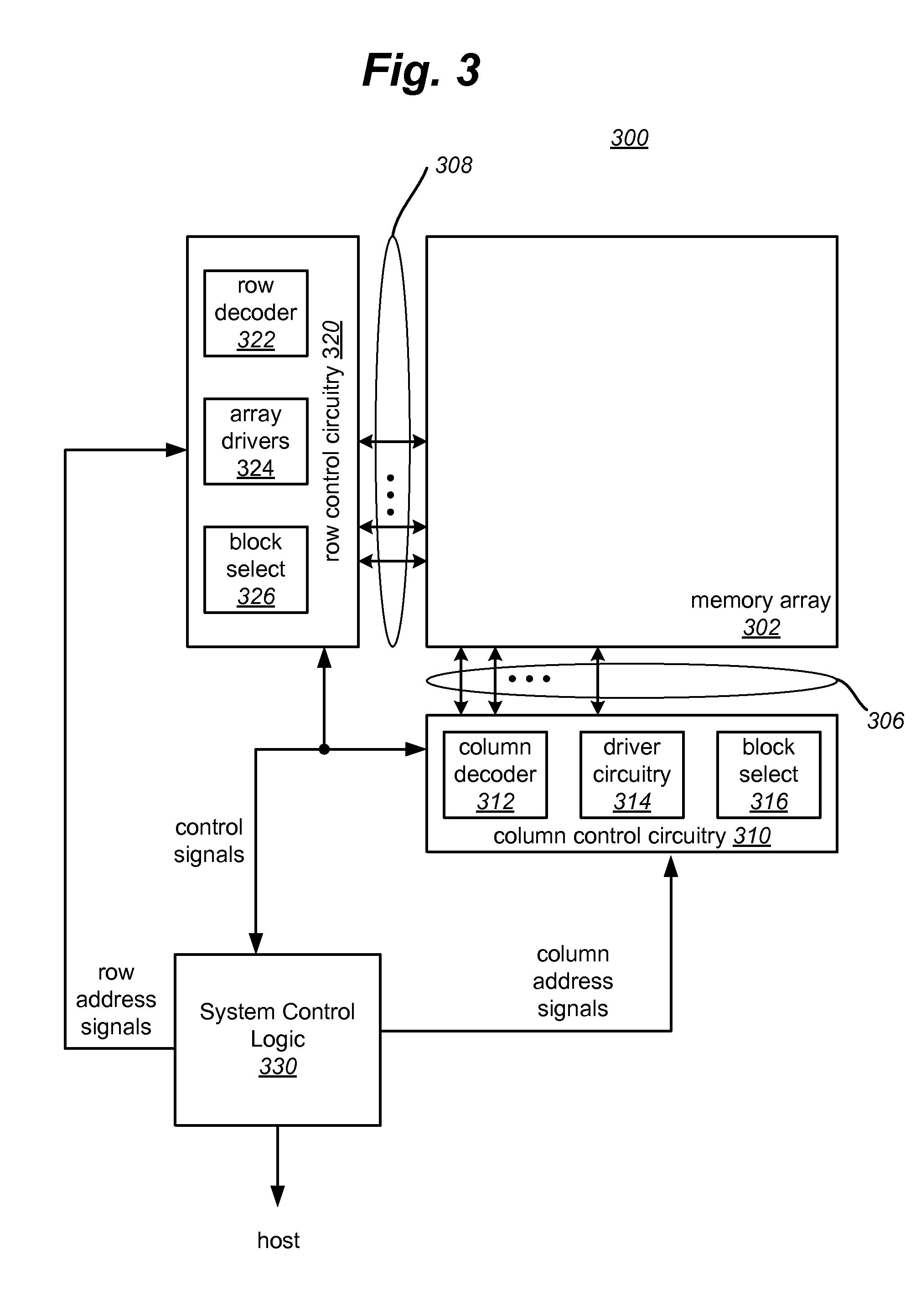
[0047]A memory system is provided that includes memory cells with one or more reversible resistivity-switching elements. Various circuits and methods are disclosed for controlling the setting and resetting of the resistance for the reversible resistance-switching elements.

Memory Cell and System

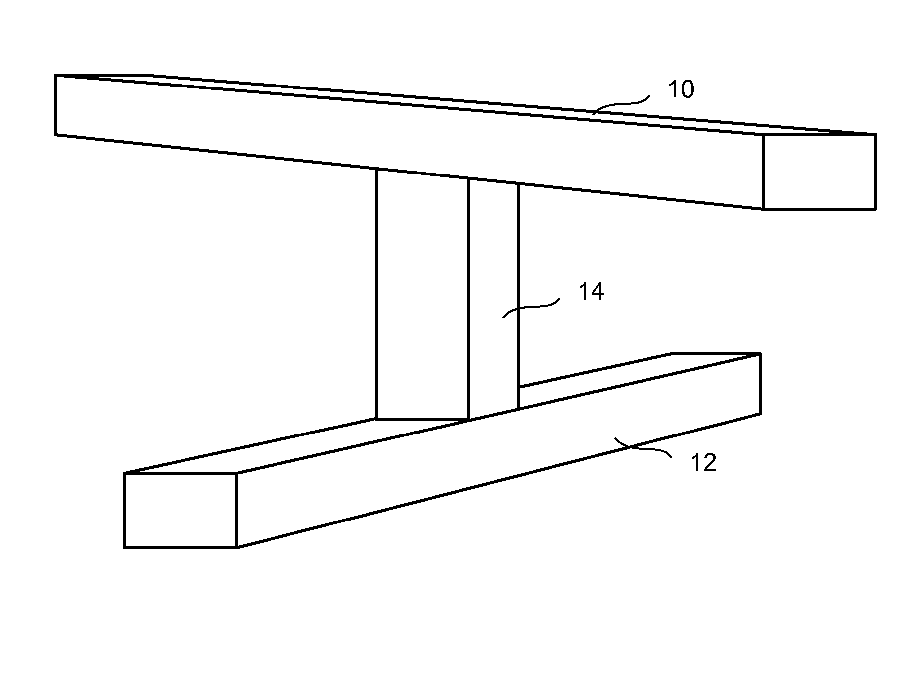
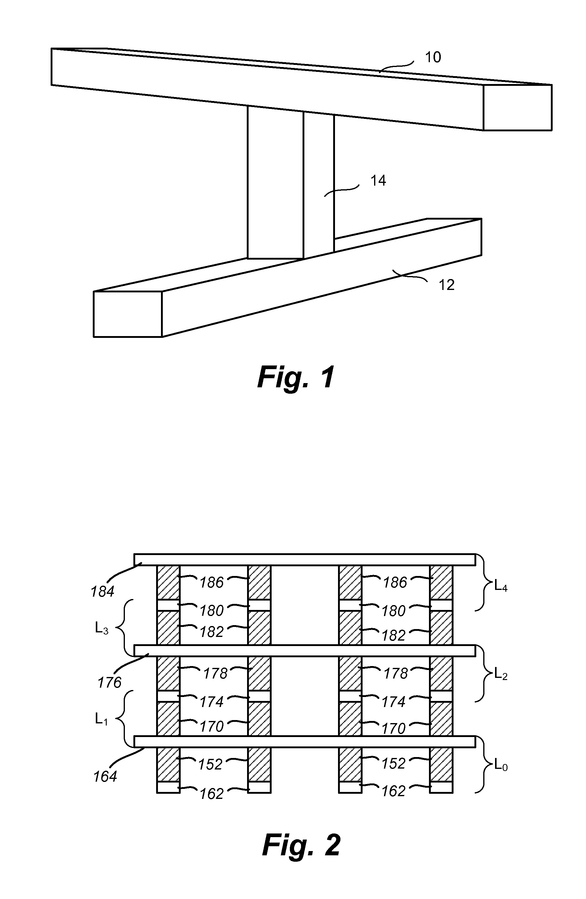
[0048]FIG. 1 is a simplified perspective view of one embodiment of a memory cell 14, which includes one reversible resistance-switching element coupled in series with a steering element, between a first conductor 10 and a second conductor 12. The steering element can take the form of any suitable device exhibiting a nonlinear conduction current characteristic, such as a diode.

[0049]The reversible resistance-switching element includes reversible resistivity-switching material having a resistivity that may be reversibly switched between two or more states. For example, the reversible resistivity-switching material may be in an initial high-resistivity state upon fabrication that is switchable to...


PUM


Abstract

A non-volatile storage apparatus comprises a set of Y lines, a set of X lines and a plurality of memory cells in communication with the set of X lines and the set of Y lines. Each memory cell of the plurality of memory cells includes a resistance element in a static resistance condition and two or more reversible resistance-switching elements. The resistance element in the static resistance condition and the two or more reversible resistance-switching elements are connected to different Y lines of the set of Y lines. The resistance element in the low resistance state and the two or more reversible resistance-switching elements are connected to a common X line of the set of X lines. One or multiple bits of data are programmed into a particular memory cell of the plurality of memory cells by causing current flow between Y lines connected to the particular memory cell.

Description

BACKGROUND[0001]1. Field[0002]The present invention relates to technology for data storage.[0003]2. Description of the Related Art[0004]A variety of materials show reversible resistance-switching behavior. These materials include chalcogenides, carbon polymers, graphitic carbon, carbon nano tubes, perovskites, and certain metal oxides and nitrides. Specifically, there are metal oxides and nitrides which include only one metal and exhibit reliable resistance switching behavior. This group includes, for example, NiO, Nb2O5, TiO2, HfO2, Al2O3, MgOx, CrO2, VO, BN, and AlN, as described by Pagnia and Sotnick in “Bistable Switching in Electroformed Metal-Insulator-Metal Device,” Phys. Stat. Sol. (A) 108, 11-65 (1988). A layer of one of these materials may be formed in an initial state, for example a relatively low-resistance state. Upon application of sufficient voltage, the material switches to a stable high-resistance state. This resistance switching is reversible such that subsequent a...

Claims


Application Information

Patent Timeline
IPC IPC(8): G11C11/00G11C7/00
CPCG11C11/5685G11C13/0007G11C13/0069G11C2213/72G11C2213/32G11C2213/34G11C2213/71G11C2013/0078G11C13/00G11C16/34
Inventor SCHEUERLEIN, ROY E.
Owner SANDISK TECH LLC
Why Eureka
Try Eureka