
Seal ring structure for integrated circuits

a technology of integrated circuits and sealing rings, which is applied in the direction of semiconductor devices, semiconductor/solid-state device details, electrical apparatus, etc., can solve the problems of adversely affecting the performance of sensitive analog and/or rf circuits, the coupling of noise between different portions of the ic, and the hurdling of implementing mixed-signal circuits, etc., to achieve the effect of improving the sealing ring structure of the integrated circuit chip and reducing the coupling of digital noise coup

Active Publication Date: 2010-11-25
MEDIATEK INC
View PDF30 Cites 4 Cited by
  • Summary
  • Abstract
  • Description
  • Claims
  • Application Information

AI Technical Summary

Benefits of technology

The present invention provides an improved seal ring structure for an integrated circuit chip that reduces digital noise coupling from a digital circuit. The seal ring structure includes a seal ring, a P+ region, and a shallow trench isolation (STI) structure. The seal ring is divided into two portions, with the second portion facing the analog and / or RF circuit block and being different in structure. The P+ region is provided in a P substrate and positioned under the second portion. The STI structure surrounds the P+ region and laterally extends underneath a conductive rampart of the second portion. This structure helps to reduce digital noise coupling and improve the performance of the integrated circuit chip.

Problems solved by technology

However, a major technical hurdle to implementing mixed-signal circuits has been the coupling of noise between different portions of the IC, for example, from the digital to the analog portions.
It has been found that the noise, such as digital noise, which, for example, may be originated from a digital power signal line such as VDD or signal pad of a digital circuit, propagates through the seal ring and adversely affects the performance of the sensitive analog and / or RF circuit.

Method used


Image

  • Seal ring structure for integrated circuits
  • Seal ring structure for integrated circuits
  • Seal ring structure for integrated circuits

Examples


Embodiment Construction

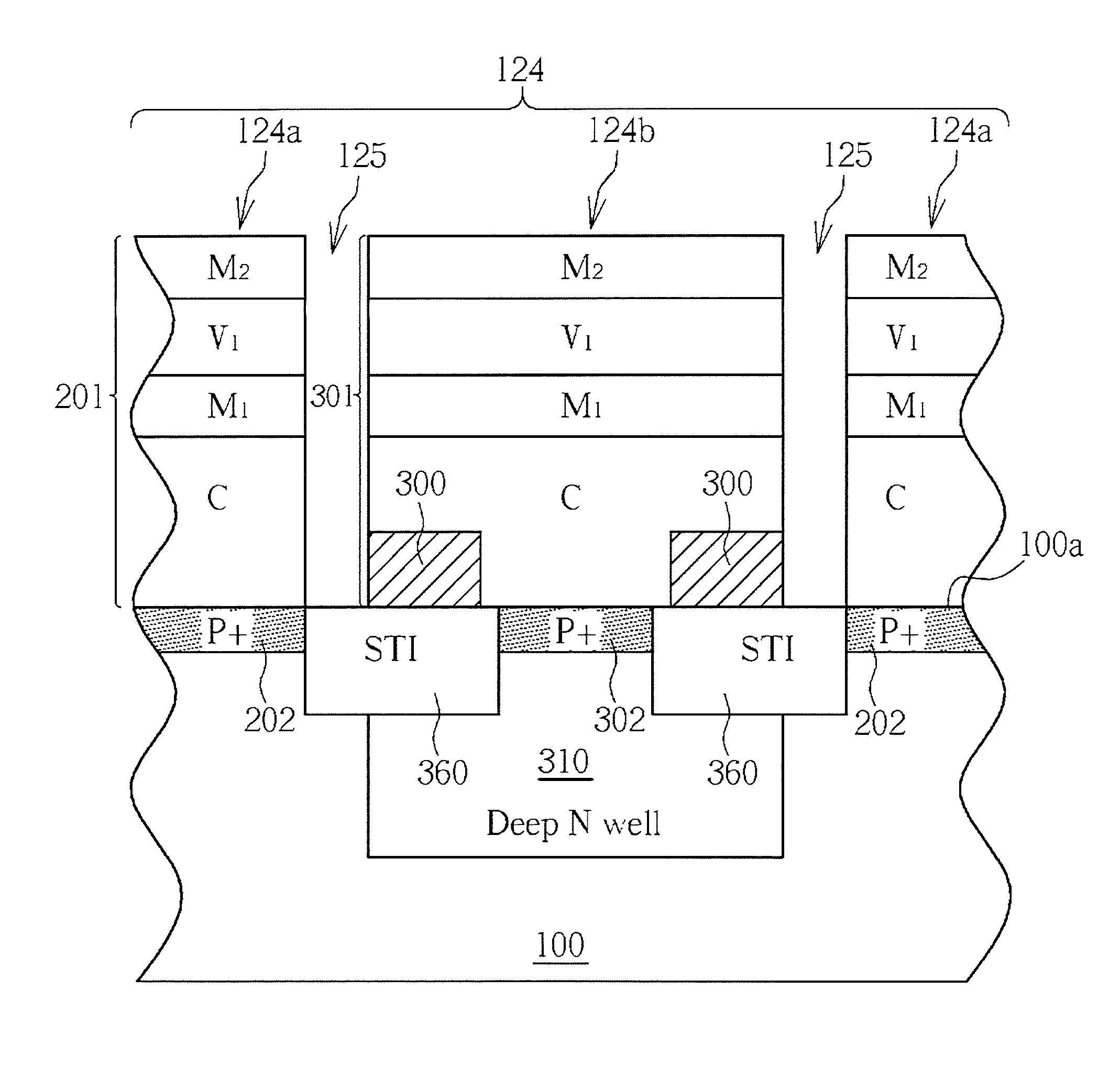
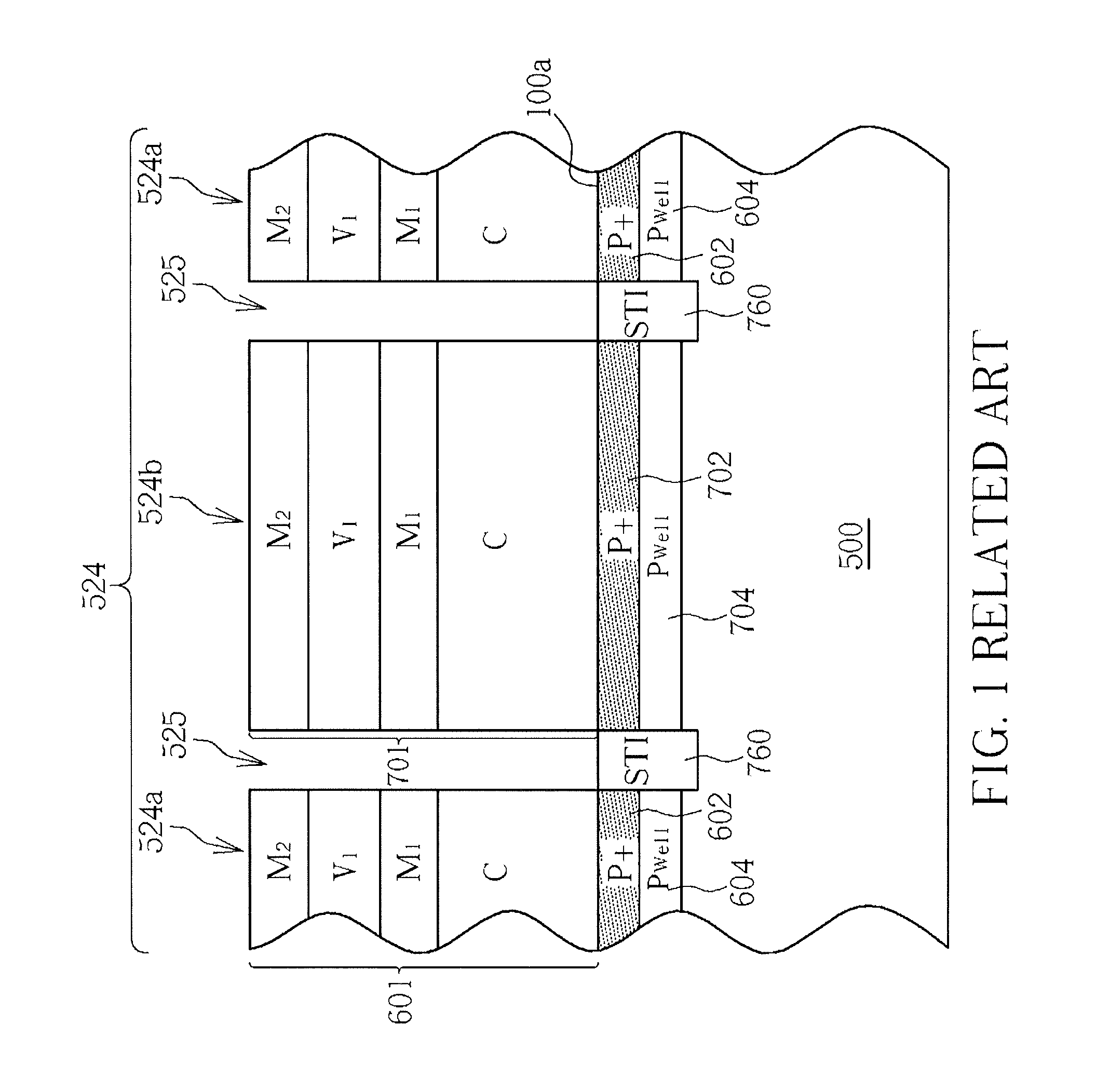
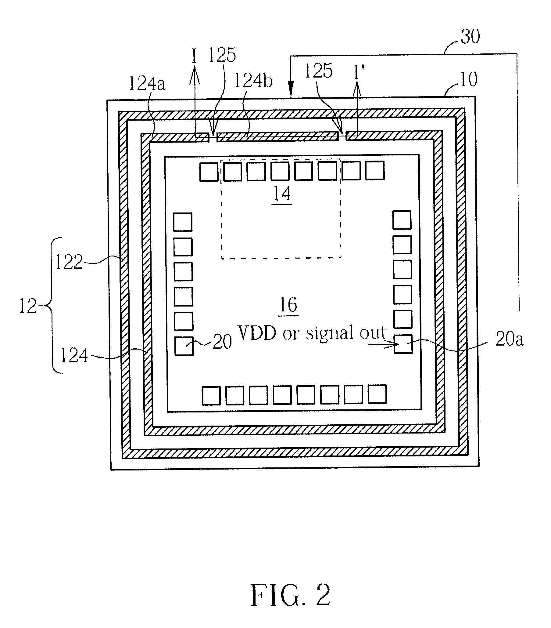
[0021]The present invention pertains to a seal ring structure for an integrated circuit chip. The number of seal ring(s) in the seal ring structure depends on requirements and is not limited to what is illustrated in the embodiments. If there is an outer seal ring, it may be a continuous ring, while an inner seal ring may be divided into at least two portions including a conductive rampart that is situated in front of a sensitive analog and / or RF circuit block of the integrated circuit chip.

[0022]A deep N well under the conductive rampart shields the analog and / or RF circuit from substrate noise, which, for example, propagates through the outer seal ring, thereby reducing the noise-coupling effects. The continuous outer seal ring keeps the moisture and corrosive substances from entering the IC. The present invention is capable of mitigating or eliminating resistive coupling noise by extending underneath a separated metal rampart portion of an inner seal ring and / or removing a P well...


PUM


Abstract

A seal ring structure for an integrated circuit includes a seal ring being disposed along a periphery of the integrated circuit and being divided into at least a first portion and a second portion, wherein the second portion is positioned facing an analog and / or RF circuit block and is different from the first portion in structure. A P+ region is provided in a P substrate and positioned under the second portion. A shallow trench isolation (STI) structure surrounds the P+ region and laterally extends underneath a conductive rampart of the second portion.

Description

CROSS REFERENCE TO RELATED APPLICATIONS[0001]The present application is a Continuation Application of U.S. patent application Ser. No. 12 / 340,737, which was filed on Dec. 21, 2008, and claimed the benefit of the filing date under 35 U.S.C. §119(e) of a Provisional U.S. Patent Application No. 61 / 057,185, filed on May 29, 2008, which is incorporated by reference herein.BACKGROUND OF THE INVENTION[0002]1. Field of the Invention[0003]The present invention related to semiconductor devices and, more particularly, to a seal ring structure for an integrated circuit that is capable of reducing substrate noise coupling.[0004]2. Description of the Prior Art[0005]Advances in fabrication technology have enabled entire functional blocks, which previously had been implemented as plural chips on a circuit board, to be integrated onto a single IC. One particularly significant development is mixed-signal circuits, which combine analog circuitry and digital logic circuitry onto a single IC.[0006]Howev...

Claims


Application Information

Patent Timeline
Patent Type & Authority Applications(United States)
IPC IPC(8): H01L29/06
CPCH01L23/5225H01L23/552H01L23/585H01L2924/0002H01L2924/00
Inventor LEE, TUNG-HSINGCHANG, TIEN-CHANGCHUNG, YUAN-HUNG
Owner MEDIATEK INC
Features
  • Generate Ideas
  • Intellectual Property
  • Life Sciences
  • Materials
  • Tech Scout
  • Unparalleled Data Quality
  • Higher Quality Content
  • 60% Fewer Hallucinations
Learn More