Nitride semiconductor laser chip

Active Publication Date: 2010-12-16
SHARP FUKUYAMA LASER CO LTD
View PDF8 Cites 9 Cited by
  • Summary
  • Abstract
  • Description
  • Claims
  • Application Information

AI Technical Summary

Benefits of technology

[0029]As described above, according to the present invention, it is possible to easily obtai

Problems solved by technology

Disadvantageously, however, it is known that when a nitride semiconductor laser chip is operated at high optical output, the resonator (cavity) facets deteriorate easily, their deterioration leading to low reliability.
Inconveniently

Method used


Image

  • Nitride semiconductor laser chip
  • Nitride semiconductor laser chip
  • Nitride semiconductor laser chip

Examples


embodiment 1

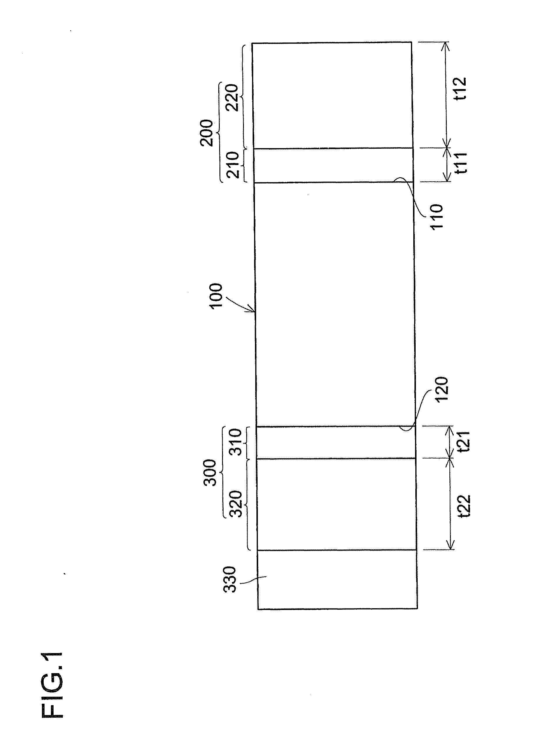
[0058]FIG. 1 is a side view schematically showing a nitride semiconductor laser chip according to a first embodiment (Embodiment 1) of the invention. FIG. 2 is a sectional view schematically showing a nitride semiconductor laser chip according to Embodiment 1 of the invention. First, with reference to FIGS. 1 and 2, the structure of a nitride semiconductor laser chip according to Embodiment 1 will be described.

[0059]As shown in FIG. 1, the nitride semiconductor laser chip according to Embodiment 1 is provided with a light-emitting structure member 100 having a pair of resonator (cavity) facets 110 and 120 opposite each other. One resonator facet 110 of the light-emitting structure member 100 is located on the light emission side, and the other resonator facet 120 is located on the light reflection side. The resonator facet 110 on the light emission side is the one provided on that side at which the reflectance at the wavelength of the laser light is lower. The light that comes out t...

example 1-1

Practical Example 1-1

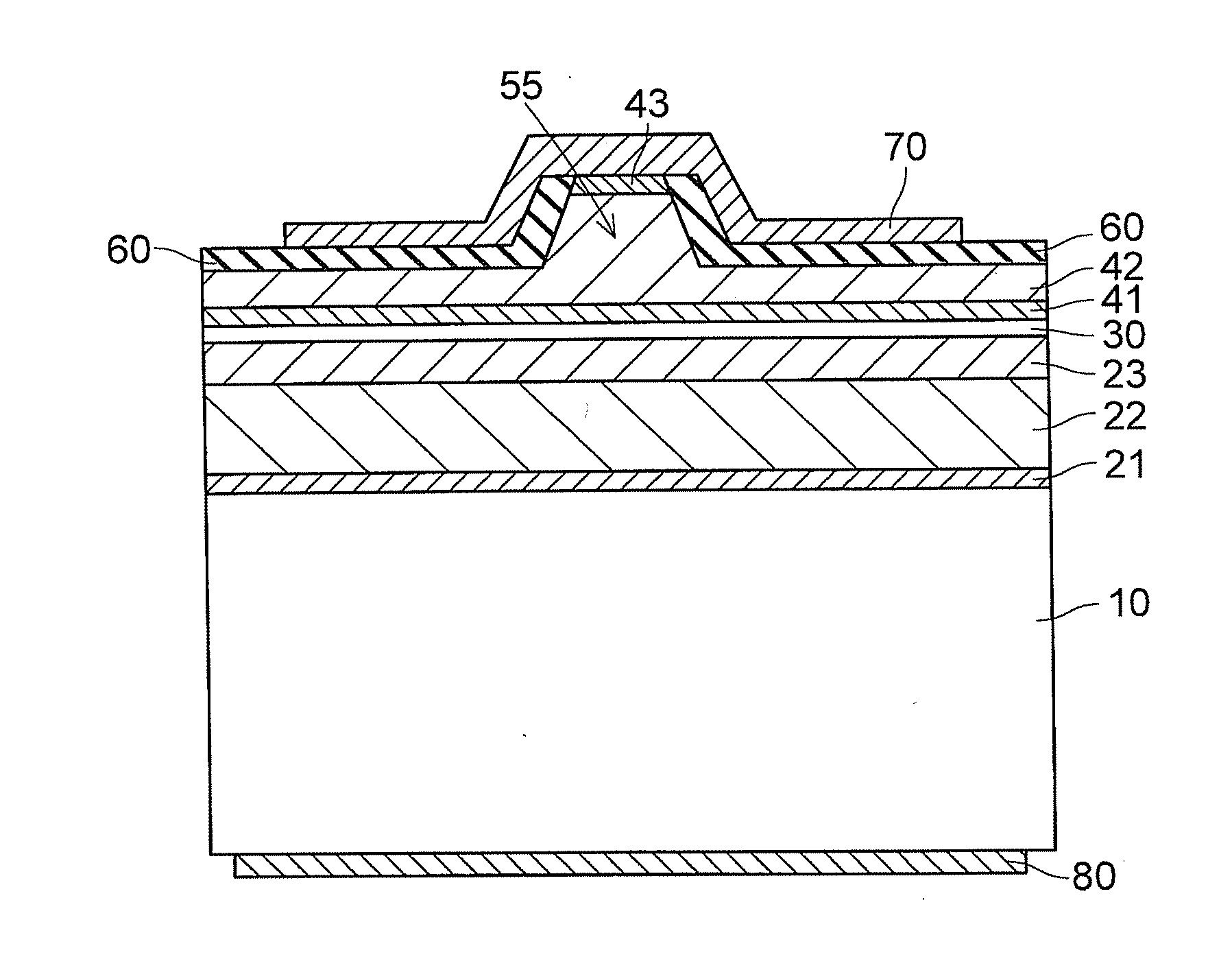
[0118]FIG. 3 is a sectional view schematically showing the structure of a nitride semiconductor laser chip according to Practical Example 1-1. FIG. 4 is a sectional view illustrating the structure of an active layer in the nitride semiconductor laser chip according to Practical Example 1-1. FIG. 5 is a side view schematically showing the nitride semiconductor laser chip according to Practical Example 1-1. First, with reference to FIGS. 2 to 5, the nitride semiconductor laser chip according to Practical Example 1-1 will be described.

[0119]In the nitride semiconductor laser chip according to Practical Example 1-1, as shown in FIG. 3, an n-type GaN substrate was used as the substrate 10. The crystal orientation of the principal growth plane of the substrate 10 was a (0001) plane.

[0120]In Practical Example 1-1, the n-type nitride semiconductor layer 20 (see FIG. 2) included an n-type GaN layer 21, an n-type clad layer, and an n-type guide layer 23, and the p-type ni...

example 1-2

Practical Example 1-2

[0152]FIG. 9 is a side view schematically showing a nitride semiconductor laser chip according to Practical Example 1-2. Next, with reference to FIGS. 4 and 9, the nitride semiconductor laser chip according to Practical Example 1-2 will be described.

[0153]In the nitride semiconductor laser chip according to Practical Example 1-2, the In composition in the quantum well layers in the active layer differed from that in Practical Example 1-1. Specifically, whereas in Practical Example 1-1 the quantum well layers 32 (see FIG. 4) were formed of In0.10Ga0.90N, in Practical Example 1-2 the quantum well layers were formed of In0.18Ga0.82N. Accordingly, in Practical Example 1-2, the lasing wavelength was 445 nm.

[0154]In Practical Example 1-2, as shown in FIG. 9, on the light-emission-side coating film 200a (200), a high-reflectance multi-layer film 230 was formed. The high-reflectance multi-layer film 230 was formed by forming two cycles of a silicon oxide (SiO2) film / a s...


PUM


Abstract

A nitride semiconductor laser chip is provided that offers sufficient reliability even at high output. The nitride semiconductor laser chip has a nitride semiconductor layer formed on a substrate, a resonator facet formed on the nitride semiconductor layer, and a coating film formed on the resonator facet and containing Ar. The coating film has, in a region contiguous with the resonator facet and in the vicinity thereof, a low-Ar region with a low Ar content and, on the side of this low-Ar region opposite from the resonator facet, a high-Ar region with a higher Ar content than the low-Ar region.

Description

[0001]This nonprovisional application claims priority under 35 U.S.C. §119(a) on Patent Application No. 2009-140083 filed in Japan on Jun. 11, 2009, the entire contents of which are hereby incorporated by reference.BACKGROUND OF THE INVENTION[0002]1. Field of the Invention[0003]The present invention relates to a nitride semiconductor laser chip, and more particularly to a nitride semiconductor laser chip having a coating film formed on a resonator facet.[0004]2. Description of Related Art[0005]Nitride semiconductor laser chips employing a nitride semiconductor are used in high-density optical disc systems with high storage capacities, specifically as a light source for reading information from and writing information to BDs (Blu-ray Discs (a registered trademark)). In such high-density optical disc systems, for increasingly fast writing to discs with increasingly large numbers of layers, nitride semiconductor laser chips with high optical output have been sought eagerly.[0006]On the...

Claims


Application Information

Patent Timeline
IPC IPC(8): H01S5/323
CPCB82Y20/00H01S5/0014H01S5/0282H01S5/22H01S5/34333
Inventor KAWAGUCHI, YOSHINOBUKAMIKAWA, TAKESHI
Owner SHARP FUKUYAMA LASER CO LTD
Why Eureka
Try Eureka