Multi-channel optical arrayed time buffer

Active Publication Date: 2010-12-30
LGS INNOVATIONS
View PDF23 Cites 0 Cited by
  • Summary
  • Abstract
  • Description
  • Claims
  • Application Information

AI Technical Summary

Benefits of technology

[0007]While the aforementioned multi-channel optical arrayed time buffer may be desirable in that it can be implemented as an integrated waveguide circuit, an aspect of this time buffer has been recognized to be disadvantageous in certain applications. In particular, in an application where lon

Problems solved by technology

While the aforementioned multi-channel optical arrayed time buffer may be desirable in that it can be implemented as an integrated waveguide circuit, an aspect of this time buffer has

Method used


Image

  • Multi-channel optical arrayed time buffer
  • Multi-channel optical arrayed time buffer
  • Multi-channel optical arrayed time buffer

Examples


Embodiment Construction

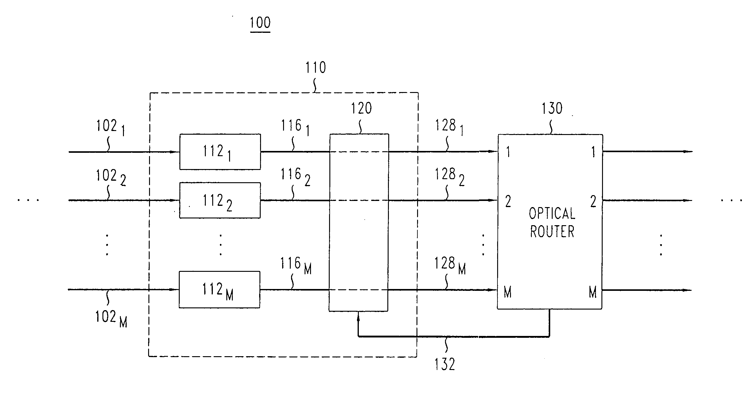
[0023]FIG. 1 shows a portion of an optical communication system 100 according to an embodiment of the invention. System 100 receives a plurality of wavelength division multiplexing (WDM) signals 1021-102M from external network components (not shown). Each of signals 1021-102M has N carrier wavelengths (λ1-λN), each modulated to carry data packets.

[0024]An optical communication system similar to system 100 is usually designed so that each of its optical elements has appropriate spectral characteristics that enable proper handling of the WDM signals that populate the system. The number of and spectral separation between the WDM components of a WDM signal are usually set based on a convention or standard. For example, the most common frequency (wavelength) grid is that used for dense WDM (WDM) and defined by a standard promulgated by the International Telecommunication Union (see ITU-T G.694.1). This grid is defined relative to 193.1 THz and extends from about 191.7 THz to about 196.1 ...


PUM


Abstract

In communications where synchronization of optical signals containing data is required, a multi-channel optical arrayed time buffer may be used. The time buffer includes multiple delay paths comprising delay elements, some of which can be shared to dispense different delays. In an embodiment, an arrayed waveguide grating (AWG) is illustratively used to route an optical signal to a first delay path, which is returnable to the AWG through the first delay path to be rerouted to a second delay path. The total delay affordable to the optical signal is a function of at least a first delay afforded by a delay element in the first delay path, and a second delay afforded by a delay element in the second delay path. In addition, without returning to the AWG, another optical signal may be routed through the second delay path alone to be afforded the second delay only.

Description

CROSS-REFERENCE TO RELATED APPLICATIONS[0001]This application is related to commonly assigned, copending U.S. patent application Ser. No. 11 / 941,191 (“the '191 application”), filed on Nov. 16, 2007, and published on May 21, 2009 as Pub. No. 2009 / 0129779; and also related to commonly assigned, copending U.S. patent application Ser. No. 11 / 941,201 (“the '201 application”), filed on Nov. 16, 2007, and published on May 21, 2009 as Pub. No. 2009 / 0129780, both of which are incorporated herein by reference in their entirety.[0002]The present invention was made with the U.S. Government support under Contract No. FA 8750-04-C-0013 awarded by the Microsystems Technology Office (MTO) of Defense Advanced Research Projects Agency (DARPA). The U.S. Government has certain rights in the invention.FIELD OF THE INVENTION[0003]The invention relates to a technique for optical communications and, more particularly, to a technique for time-buffering optical signals.BACKGROUND OF THE INVENTION[0004]This s...

Claims


Application Information

Patent Timeline
IPC IPC(8): H04J14/00
CPCH04Q11/0005H04Q2011/0016H04Q2011/002H04Q2011/0032H04Q2011/0045
Inventor BERNASCONI, PIETRO
Owner LGS INNOVATIONS
Why Eureka
Try Eureka