Correction circuit and display device

a display device and correction circuit technology, applied in the field of correction circuits and display devices, can solve the problems of difficult to accurately perform the correction for every pixel, etc., to suppress display non-uniformity with accuracy, reduce storage capacity, and reduce the effect of pixel brightness

Inactive Publication Date: 2011-02-10
IETOMI KUNIHIKO
View PDF3 Cites 11 Cited by
  • Summary
  • Abstract
  • Description
  • Claims
  • Application Information

AI Technical Summary

Benefits of technology

[0028]According to the embodiment of the present invention, luminance non-uniformity may be corrected in every pixel while keeping the storage capacity of the memory small, being able to suppress display non-uniformity with accuracy.

Problems solved by technology

However, in the technique disclosed in Japanese Unexamined Patent Application Publication No. 2004-264793, since the display panel is divided into small areas and a trend of the whole of the display panel is calculated by a small area unit, it is difficult to accurately perform correction for every pixel.
Further, though a storage capacity of the memory can be kept small in the case of the correction in the small area unit, it is still difficult to accurately perform the correction for every pixel.

Method used


Image

  • Correction circuit and display device
  • Correction circuit and display device
  • Correction circuit and display device

Examples


Embodiment Construction

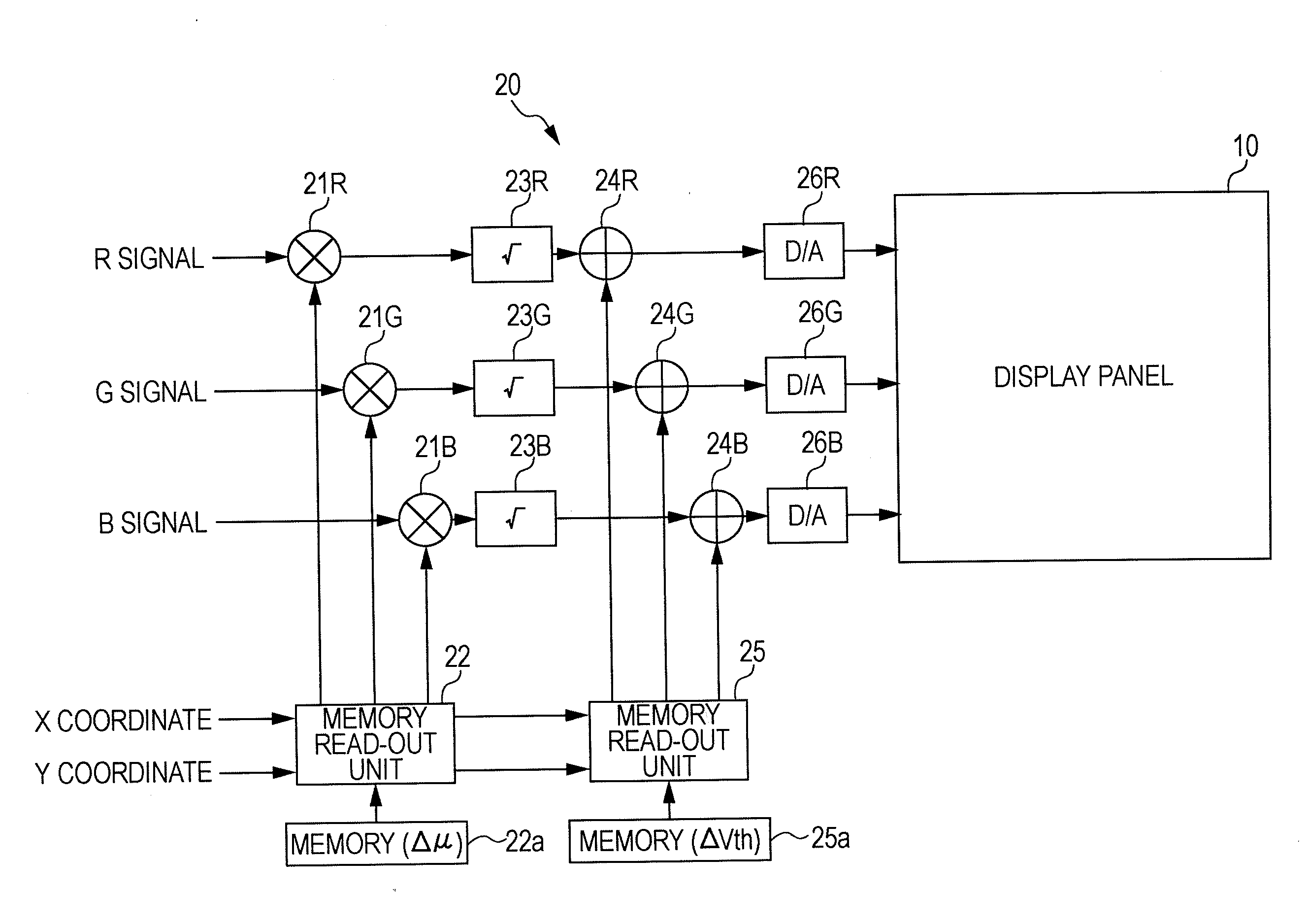
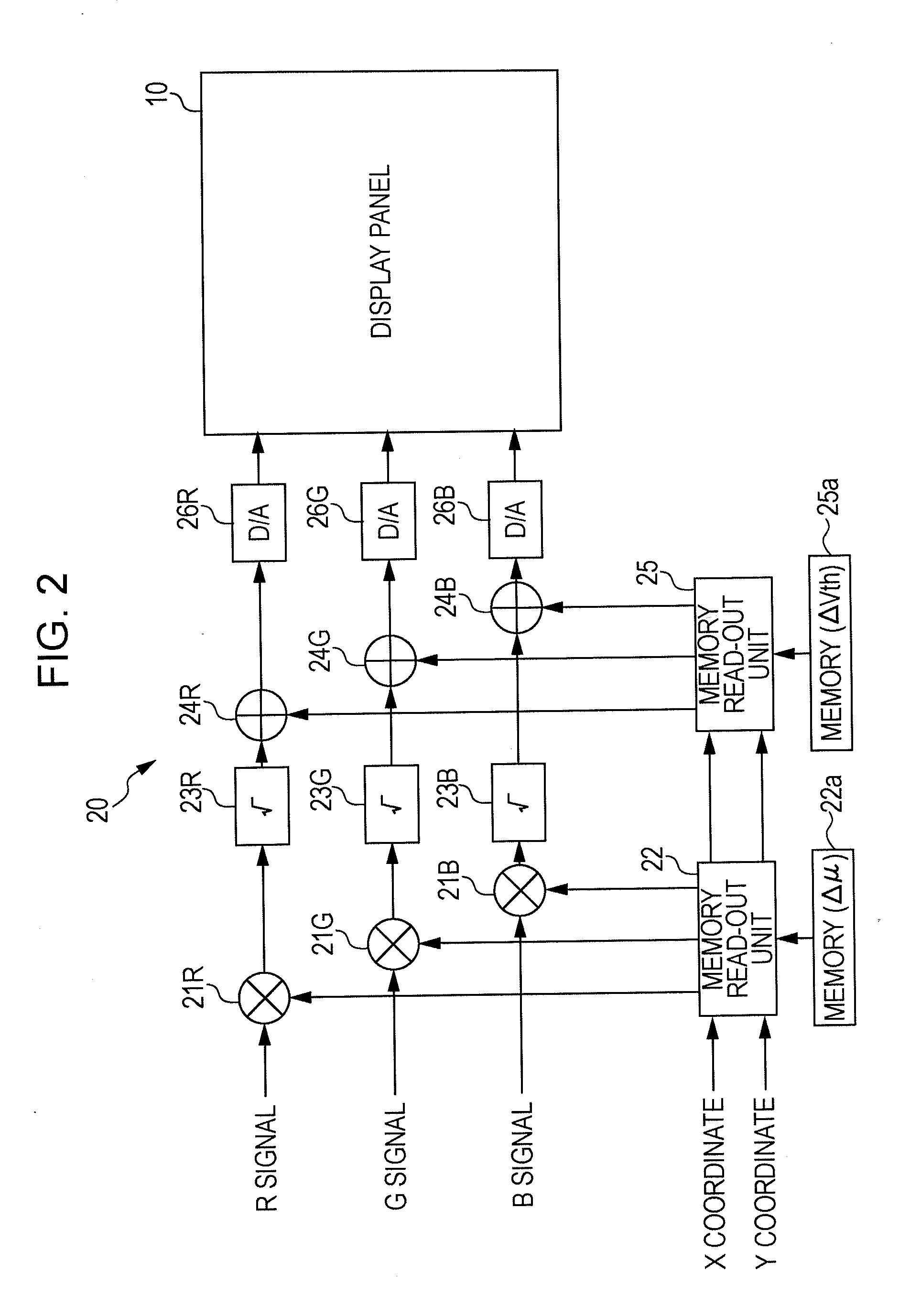
[0036]Embodiments of the present invention will now be described with reference to the accompanying drawings in the following order.[0037]1. Embodiment (a correlation table: an example of a case where ΔVth is produced from Δμ)[0038]2. Another embodiment (a correlation table: an example of a case where Δμ is produced from ΔVth)

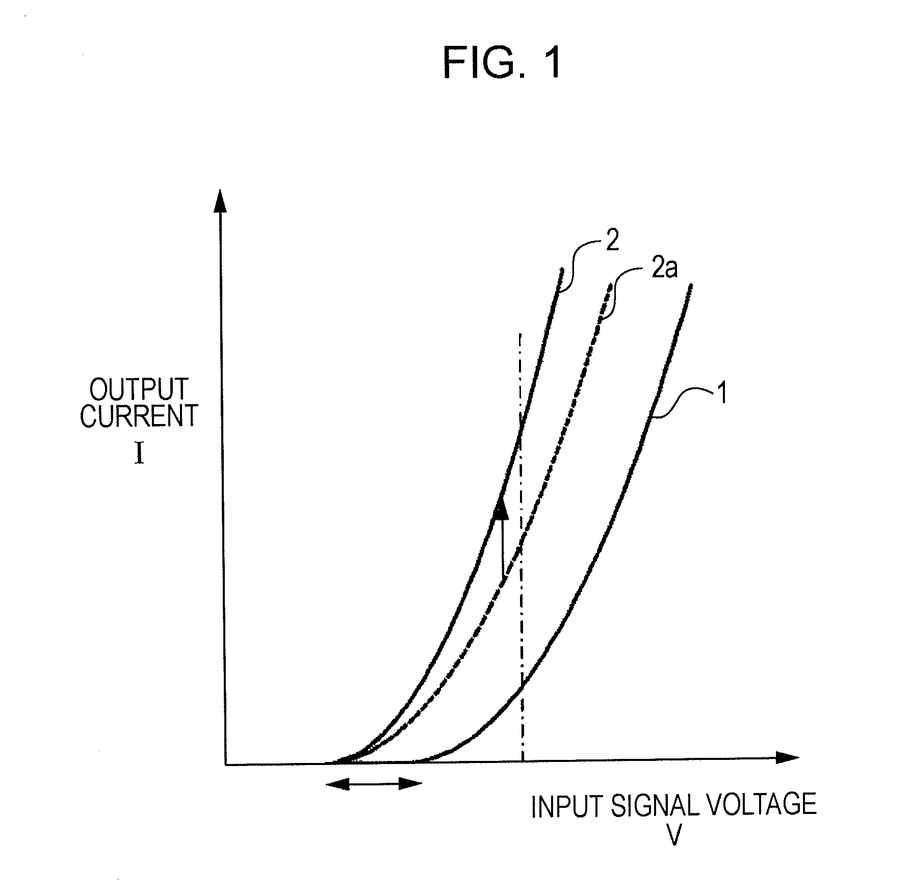
[0039]According to Expression 1 above, in an active matrix TFT panel based on a current driving method, a drain current (output current I) of a driving transistor in a pixel circuit is proportional to mobility μ and is proportional to the square of a difference between a gate applied voltage Vgs and a threshold voltage Vth. That is, accuracy of the drain current (output current I) of a driving transistor depends on accuracy of the mobility μ and accuracy of the square of the difference between the gate applied voltage Vgs and the threshold voltage Vth.

[0040]In the light of the such characteristic of the output current of the driving transistor, in an embodiment...


PUM


Abstract

A correction circuit includes a memory that stores a mobility correction value or a threshold voltage correction value for correcting luminance non-uniformity for every pixel, a memory read-out unit that reads out the mobility correction value or the threshold voltage correction value from the memory, a correlation table that produces a threshold voltage correction value or a mobility correction value from the other one of the mobility correction value and the threshold voltage correction value on the basis of a correlation between mobility and a threshold voltage, a mobility correction unit correcting an input signal for every pixel by using the mobility correction value supplied from the memory read-out unit or the correlation table, and a threshold voltage correction unit correcting the input signal that is corrected at the mobility correction unit, by using the threshold voltage correction value supplied from the memory read-out unit or the correlation table.

Description

BACKGROUND OF THE INVENTION[0001]1. Field of the Invention[0002]The present invention relates to a correction circuit and a display device that correct display non-uniformity occurring in a display device in which display elements are arranged in matrix.[0003]2. Description of the Related Art[0004]In an organic EL display device, organic EL elements, which are self-emissive elements, are used as pixels. A luminance level (gradation) of each of the organic EL elements, that is, light emitting elements, arranged in matrix can be controlled by a current flowing in the elements. Thus the organic EL display device is a current controlled device (current drive method) and therefore greatly differs from a voltage controlled device such as a liquid crystal display device.[0005]Organic EL display devices employ a passive matrix method or an active matrix method as a driving method thereof. In recent years, organic EL display devices employing the active matrix method have been extensively de...

Claims


Application Information

Patent Timeline
Patent Type & Authority Applications(United States)
IPC IPC(8): G09G5/10
CPCG09G2300/0819G09G3/3233G09G2320/043G09G2320/029G09G2320/0285
Inventor IETOMI, KUNIHIKO
Owner IETOMI KUNIHIKO
Why Eureka
Try Eureka