Liquid crystal display device

a liquid crystal display and display device technology, applied in static indicating devices, non-linear optics, instruments, etc., can solve the problems of display failure, high design cost, luminance degradation,

Active Publication Date: 2020-08-11
SHARP KK
View PDF5 Cites 0 Cited by
  • Summary
  • Abstract
  • Description
  • Claims
  • Application Information

AI Technical Summary

Benefits of technology

[0005]Therefore, it is desirable to provide a liquid crystal display device that can reduce design cost and suppress luminance degradation and display failure.

Problems solved by technology

Therefore, the time-division drive type liquid crystal display device has to be manufactured by newly designing a mask, so that design cost is high.
However, when simply connecting three sub-pixel electrodes together, liquid crystal alignment directions are largely changed from a state before the sub-pixel electrodes are connected together, so that there is a problem that luminance degradation and display failure of the liquid crystal display device occur.

Method used


Image

  • Liquid crystal display device
  • Liquid crystal display device
  • Liquid crystal display device

Examples


first embodiment

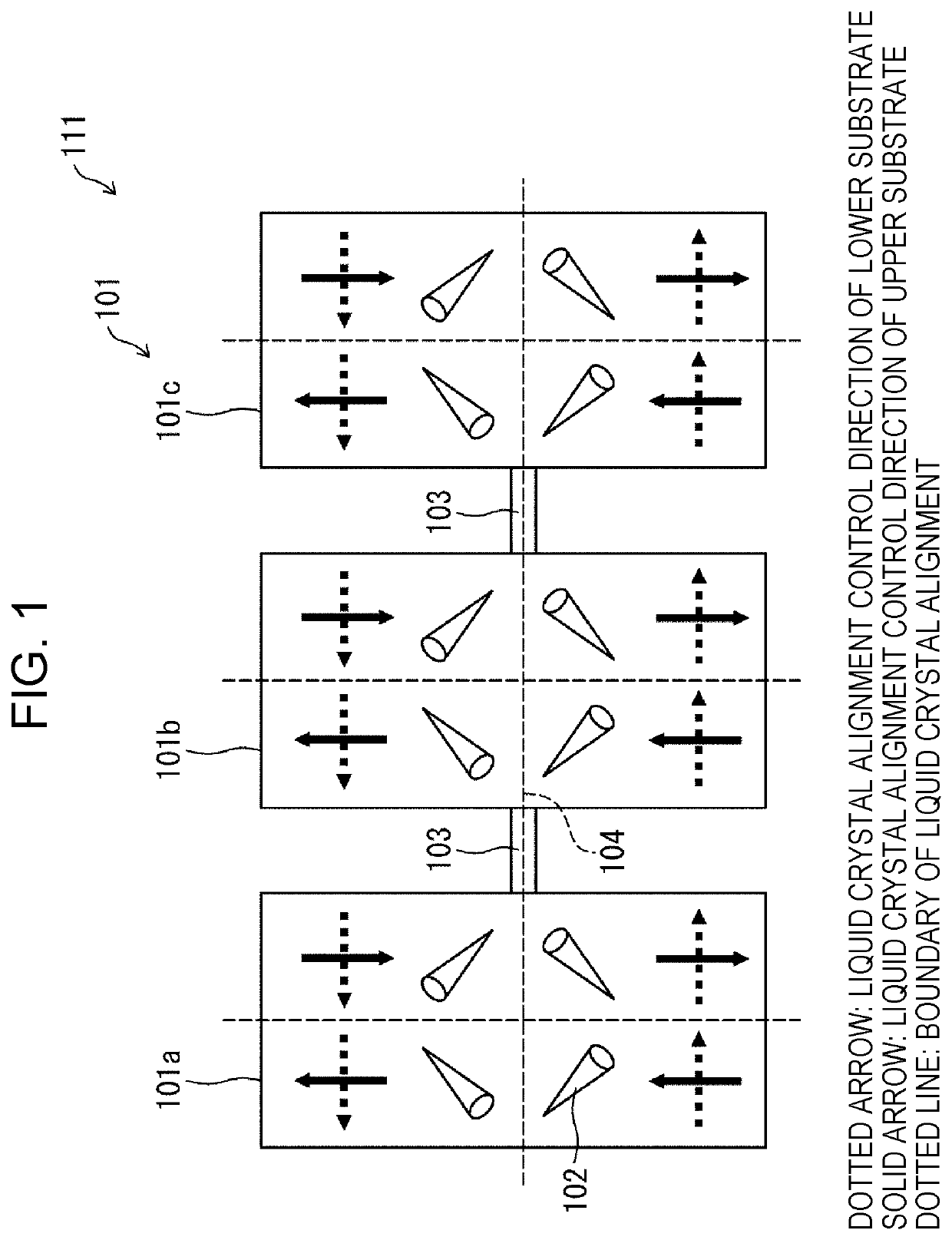
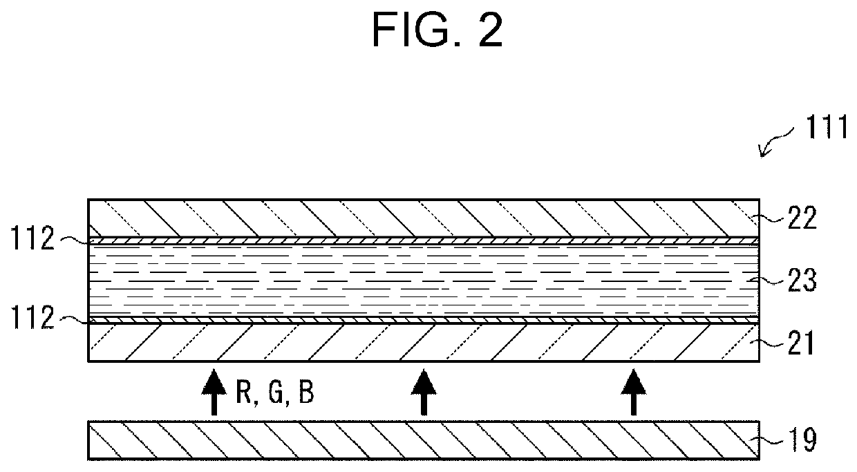
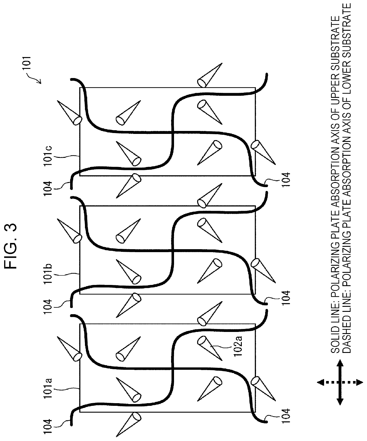
[0031]An embodiment of the present disclosure will be described below with reference to the drawings. FIG. 1 is an explanatory diagram of a liquid crystal display panel 111 having an pixel electrode 101 formed by connecting three divided sub-pixel (picture element) electrodes 101a to 101c of a liquid crystal display device of the present embodiment. FIG. 2 is a schematic vertical cross-sectional view of the liquid crystal display panel 111 included in the liquid crystal display device of the present embodiment.

[0032]As shown in FIG. 2, in the liquid crystal display panel 111, a TFT substrate (active matrix substrate) 21 and a counter substrate 22 are arranged facing each other, and a liquid crystal layer 23 is provided between the TFT substrate 21 and the counter substrate 22. An alignment film 112 is provided to an inner surface of each of the TFT substrate 21 and the counter substrate 22. Reference numeral 19 denotes a backlight device. The configuration of the liquid crystal disp...

second embodiment

[0053]Another embodiment of the present disclosure will be described with reference to the drawings. For convenience of description, members that have the same functions as those of the members described in the above embodiment will be denoted by the same reference numerals, and descriptions thereof will be omitted.

[0054]FIG. 6A is an explanatory diagram of a liquid crystal display panel 131 having an pixel electrode 121 formed by connecting three divided sub-pixel electrodes (picture elements) 121a to 121c of a liquid crystal display device of the present embodiment, and FIG. 6B is an explanatory diagram showing a state where structures 143 on a counter substrate 22 (see FIG. 2) are removed from the liquid crystal display panel 131 shown in FIG. 6A.

[0055]For convenience, FIG. 6A shows the liquid crystal alignment directions (alignment directions of the liquid crystal molecules 102a) before the sub-pixel electrodes 121a to 121c are connected by the interelectrode connection portions...

third embodiment

[0068]Further another embodiment of the present disclosure will be described below with reference to the drawings. For convenience of description, members that have the same functions as those of the members described in the above embodiments will be denoted by the same reference numerals, and descriptions thereof will be omitted.

[0069]FIG. 9A is an explanatory diagram of a liquid crystal display panel 132 having an pixel electrode 121 formed by connecting three divided sub-pixel electrodes (picture elements) 121a to 121c of a liquid crystal display device of the present embodiment, and FIG. 9B is an explanatory diagram showing a state where structures 143 on a counter substrate 22 (see FIG. 2) are removed from the liquid crystal display panel 132 shown in FIG. 9A.

[0070]In the same manner as FIG. 6A, for convenience, FIG. 9A shows the liquid crystal alignment directions (alignment directions of the liquid crystal molecules 102a) before the sub-pixel electrodes 121a to 121c are conne...


PUM

PropertyMeasurementUnit
widthaaaaaaaaaa
widthaaaaaaaaaa
frame timeaaaaaaaaaa

Abstract

A liquid crystal display device includes sub-pixel electrodes respectively provided to three sub-pixels, and an interelectrode connection portion that connects sub-pixel electrodes adjacent to each other among the sub-pixel electrodes. The interelectrode connection portion is provided in a position where boundaries of liquid crystal alignment directions of sub-pixels adjacent to each other are connected.

Description

BACKGROUND1. Field[0001]The present disclosure relates to a liquid crystal display device that can be used as, for example, a time-division drive type liquid crystal display device.2. Description of the Related Art[0002]Conventionally, for example, a time-division drive type liquid crystal display device of FSC (Field Sequential Color) system is known. As described in Japanese Patent No. 4579204, the liquid crystal display device writes a signal by scanning three gate lines at a time.[0003]However, as described in Japanese Patent No. 4579204, in a configuration where a gate driver drives three gate lines at the same time, a region where the gate lines are drawn is three times the region in a configuration where the gate driver drives the gate lines one by one. Therefore, for example, when designing a time-division drive type liquid crystal display device where the gate driver drives three gate lines at the same time, a large design change is required for a design of a liquid crystal...

Claims


Application Information

Patent Timeline
Patent Type & Authority Patents(United States)
IPC IPC(8): G09G3/36G02F1/1343G02F1/13357
CPCG09G3/3648G02F1/1336G09G3/3607G02F1/134309G09G2310/0235G09G2300/0426G09G2300/0447G09G2300/0443G02F1/133753G02F1/136286G02F1/13373G02F1/134345
Inventor SASAKI, TAKAHIROYOSHIDA, HIDEFUMIHANAOKA, KAZUTAKANAKAMURA, KIMIAKI
Owner SHARP KK
Why Eureka
Try Eureka