Optical Touch Device and Locating Method thereof, and Linear Light Source Module

a technology of optical touch and locating method, which is applied in the field of optical touch devices and locating methods thereof, can solve the problems of inability to accurately calculate the coordinates of the touch point b, the conventional optical touch device b>100/b>/i>a is unsuitable for dual-touch devices or multi-touch devices, and achieves the effect of effective and available optical information

Inactive Publication Date: 2011-03-17
PIXART IMAGING INC
View PDF33 Cites 37 Cited by
  • Summary
  • Abstract
  • Description
  • Claims
  • Application Information

AI Technical Summary

Benefits of technology

[0028]In the optical touch device of the present invention, the third light guide component and the fourth light guide component of the light guide module are the mirror light guide components, and the first light emitting component and the second light emitting component are configured for emitting light alternately. When the third light guide component provides a mirror function, the fourth light guide provides a light guide function. When the fourth light guide provides a mirror function, the third light guide component provides a light guide function. Thus, the image detecting module can detect effective and available optical information, and thereby avoiding the problem of the blind zone. In addition, the locating method of the optical touch device of the present invention includes the step of controlling the first light emitting component and the second

Problems solved by technology

Thus, the coordinates of the touch point B can not be calculated accurately.
Thus, the complexity of calculating the coordinates of the two touch points

Method used


Image

  • Optical Touch Device and Locating Method thereof, and Linear Light Source Module
  • Optical Touch Device and Locating Method thereof, and Linear Light Source Module
  • Optical Touch Device and Locating Method thereof, and Linear Light Source Module

Examples


Embodiment Construction

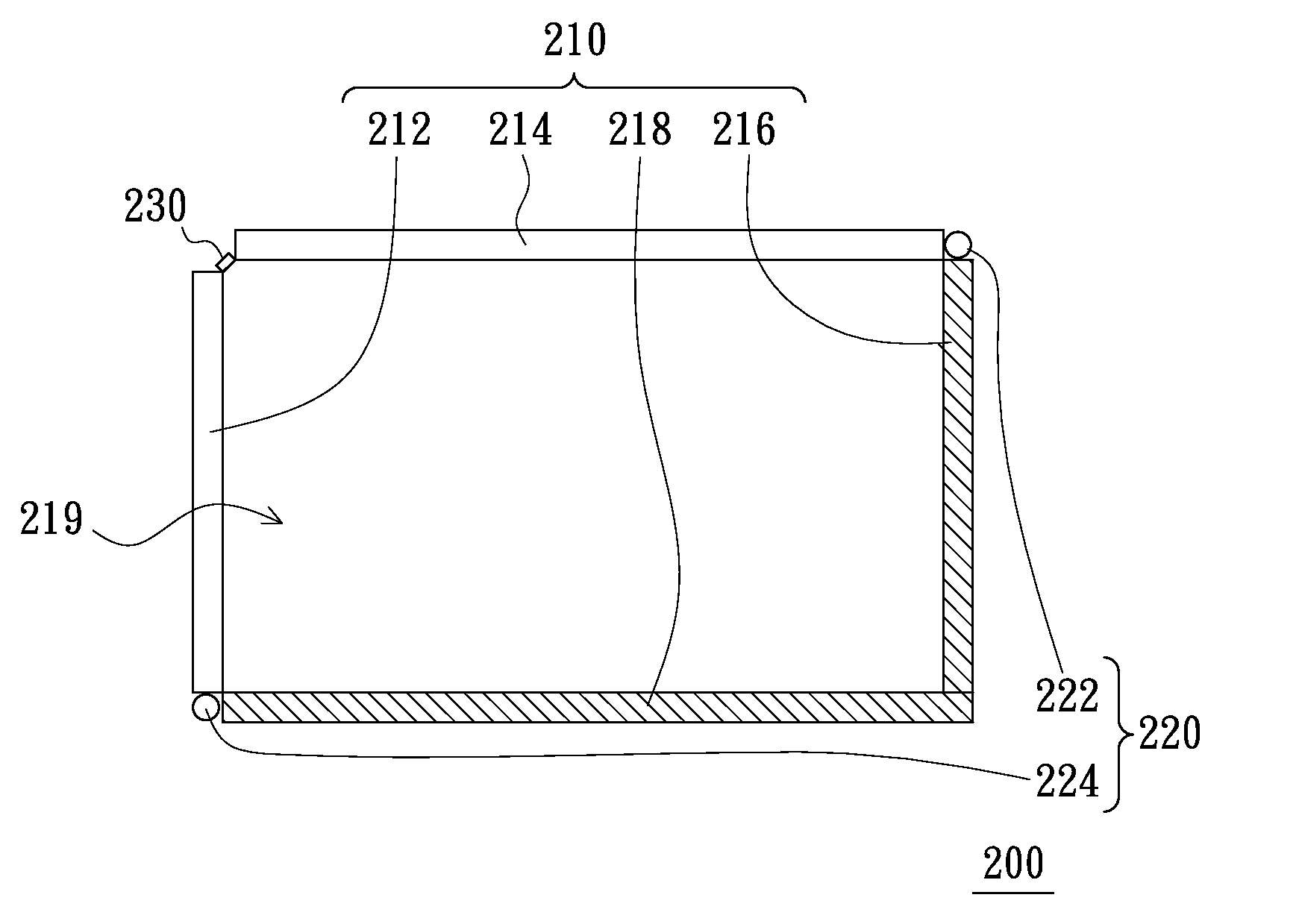
[0042]FIG. 3 is a schematic view of an optical touch device in accordance with a first embodiment of the present invention. Referring to FIG. 3, in the present embodiment, the optical touch device 200 includes a light guide module 210, a light source module 220 and an image detecting module 230. The light guide module 210 includes a first light guide component 212, a second light guide component 214, a third light guide component 216 and a fourth light guide component 218 arranged along four sides of a rectangle. The first light guide component 212, the second light guide component 214, the third light guide component 216 and the fourth light guide component 218 defines a detecting area 219 therebetween. The first light guide component 212 faces to the third light guide component 216, and the second light guide component 214 faces to the fourth light guide component 218. The light source module 220 is configured for providing light to the third light guide component 216 and the four...


PUM


Abstract

An optical touch device includes a light guide module including a first light guide component, a second light guide component, a third light guide component and a fourth light guide component, a light source module including a first light emitting component and a second light emitting component for emitting light alternately and an image detecting module disposed between two neighboring ends of the first light guide component and the second light guide component. The third light guide component and the fourth light guide component are mirror light guide components. A field of view of the image detecting module covers the third light guide component and the fourth light guide component. The optical touch device can avoid a blind zone and can be used as a dual-touch device or a multi-touch device. A locating method and a linear source module are also provided.

Description

CROSS-REFERENCE TO RELATED APPLICATIONS[0001]This application is based upon and claims the benefit of priority from the prior Taiwanese Patent Application No. 098131423, filed Sep. 17, 2009, the entire contents of which are incorporated herein by reference.BACKGROUND[0002]1. Field of the Invention[0003]The present invention relates to a touch device, and particularly to an optical touch device and a locating method thereof, and a linear light source module.[0004]2. Description of the Related Art[0005]Nowadays, a touch function has been one of necessary functions of many electronic devices. A touch device is an important component to achieve the touch function. Generally, a familiar type of the touch device is, for example, a resistive touch device, a capacitive touch device or an optical touch device. The electronic devices can be equipped with various touch devices in accordance with the various demands.[0006]FIG. 1 is a schematic view of a conventional optical touch device. Referr...

Claims


Application Information

Patent Timeline
IPC IPC(8): G06F3/042
CPCG06F3/0428G02B6/0096G02B6/0001
Inventor CHENG, HSIN-CHILIN, CHO-YI
Owner PIXART IMAGING INC
Why Eureka
Try Eureka