Touch panel and display device using the same
- Summary
- Abstract
- Description
- Claims
- Application Information
AI Technical Summary
Benefits of technology
Problems solved by technology
Method used
Image

Examples
first embodiment
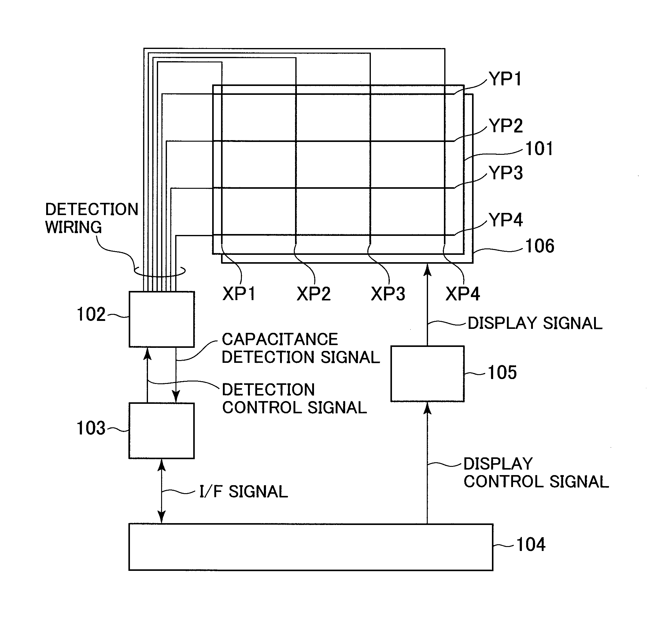
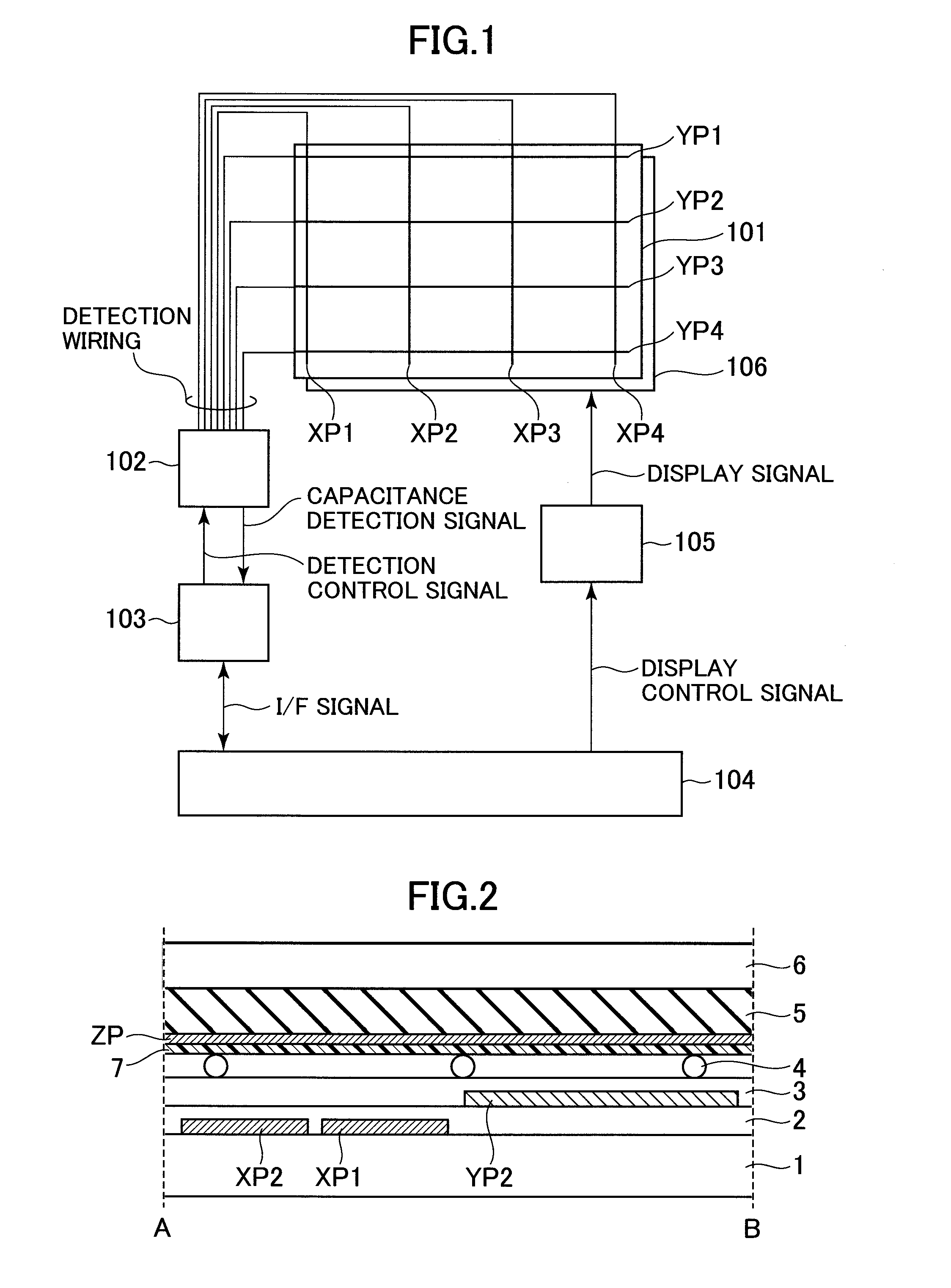
[0048]FIG. 1 is a system configuration diagram for illustrating a schematic configuration of a display device according to a first embodiment of the present invention. In the following, with reference to FIG. 1, an overall configuration of the display device according to the first embodiment is described.
[0049]FIG. 1 illustrates a touch panel 101 of capacitive type (more specifically, capacitive coupling type), which serves as an input device for use in the display device according to the first embodiment of the present invention. The touch panel 101 includes X electrodes XP and Y electrodes YP for capacitance detection. The first embodiment is described as an exemplary case where, for example, four X electrodes (XP1 to XP4) and four Y electrodes (YP1 to YP4) are provided. However, each of the numbers of the X electrodes and the Y electrodes is not limited to four. The touch panel 101 is disposed on a front surface of a display panel 106. Accordingly, in the display device according...
second embodiment
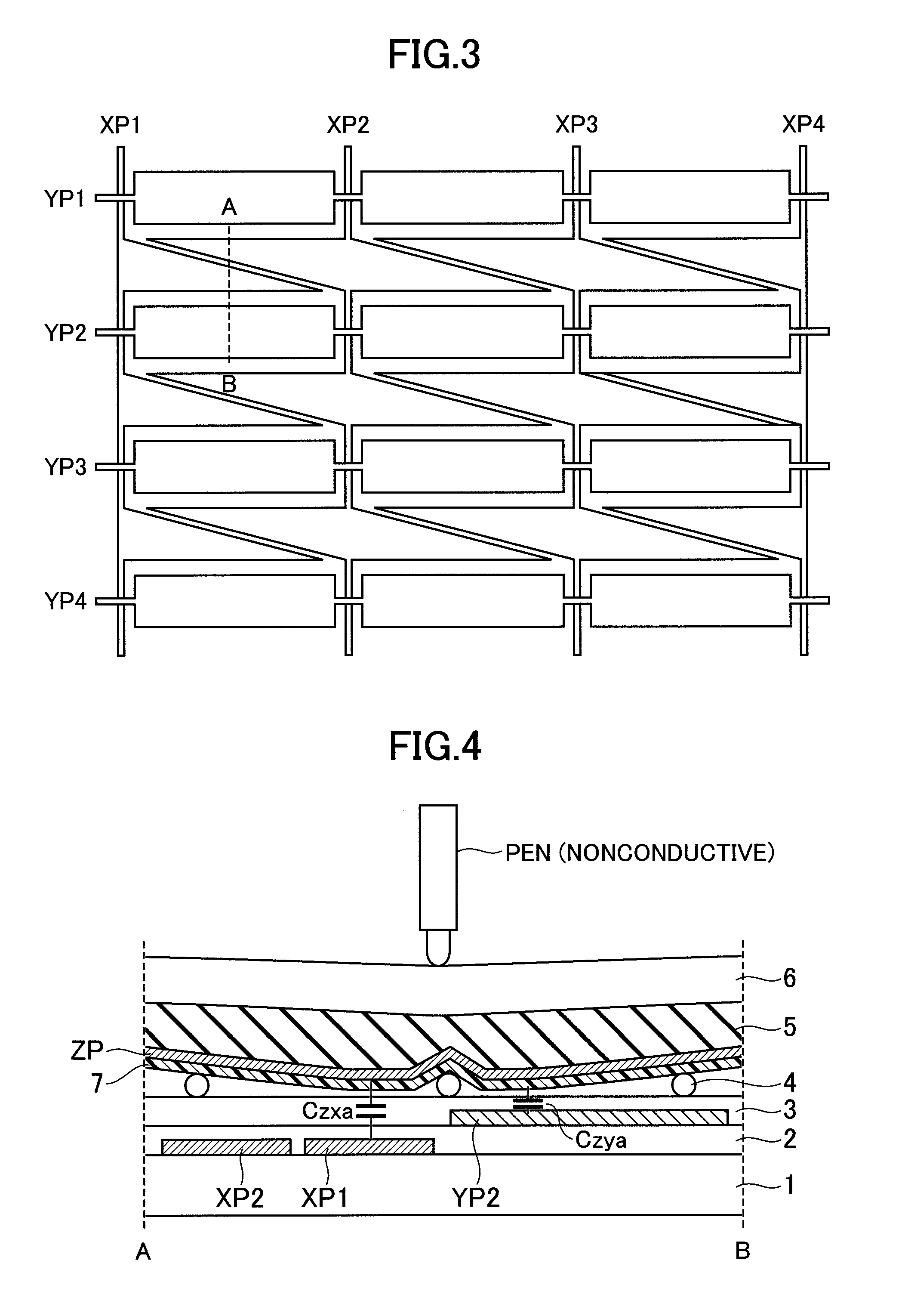
[0087]FIG. 9 is a sectional view illustrating an electrode structure of a touch panel 101 of a display device according to a second embodiment of the present invention. Here, the sectional view illustrated in FIG. 9 corresponds to the sectional view of FIG. 2 of the first embodiment. In particular, the touch panel 101 according to the second embodiment is similar in configuration to the touch panel 101 according to the first embodiment, except for the position for forming the antireflective film. Accordingly, the second embodiment is similar to the first embodiment in terms of material and property of each layer. In the following, the configuration of an antireflective film 12 is described in detail. Note that, the display panel 106 and the touch panel 101 are laminated in a manner similar to that of the first embodiment.
[0088]As is apparent from FIG. 9, the touch panel 101 according to the second embodiment of the present invention has a configuration in which the X electrode (tran...
third embodiment
[0095]FIG. 11 is a sectional view illustrating an electrode structure of a touch panel 101 of a display device according to a third embodiment of the present invention. Here, the sectional view illustrated in FIG. 11 corresponds to the sectional view of FIG. 2 of the first embodiment. In particular, the touch panel 101 according to the third embodiment is similar in configuration to the touch panel 101 according to the first embodiment, except for the position for forming the antireflective film. Accordingly, the third embodiment is similar to the first embodiment in terms of material and property of each layer. In the following, the configuration of the antireflective film is described in detail. Note that, the display panel 106 and the touch panel 101 are laminated in a manner similar to that of the first embodiment.
[0096]As is apparent from FIG. 11, the touch panel 101 according to the third embodiment of the present invention has a configuration in which the X electrode (transpa...
PUM
 Abstract
Description
Claims
Application Information
 - Generate Ideas
- Intellectual Property
- Life Sciences
- Materials
- Tech Scout
- Unparalleled Data Quality
- Higher Quality Content
- 60% Fewer Hallucinations
Browse by: Latest US Patents, China's latest patents, Technical Efficacy Thesaurus, Application Domain, Technology Topic, Popular Technical Reports.
© 2025 PatSnap. All rights reserved.Legal|Privacy policy|Modern Slavery Act Transparency Statement|Sitemap|About US| Contact US: help@patsnap.com