
Integrated circuit chip with pyramid or cone-shaped conductive pads for flexible c4 connections and a method of forming the integrated circuit chip

a technology of integrated circuit chips and conductive pads, which is applied in the direction of electrical equipment, semiconductor devices, semiconductor/solid-state device details, etc., can solve the problems of stress-related cracks in the c4 connection and/or the integrated circuit chip(s), chip failure, and stress-related cracks that can increase exponentially

Inactive Publication Date: 2011-06-16
GLOBALFOUNDRIES INC
View PDF16 Cites 38 Cited by
  • Summary
  • Abstract
  • Description
  • Claims
  • Application Information

AI Technical Summary

Problems solved by technology

Unfortunately, during chip operation, stress-related cracks in the C4 connections and / or the integrated circuit chip(s) can form due to a mismatch in thermal expansion (e.g., between the integrated circuit chip and the chip carrier in a flip-chip assembly and between the multiple integrated circuit chips in a stacked chip assembly).
Such stress-related cracks can result in chip failure.
Furthermore, such stress-related cracks can increase exponentially with the use of an organic laminate substrate as the chip carrier in a flip-chip assembly, with the use of lead-free solder material and / or with smaller pitch C4 connections (i.e., with greater C4 connection density).

Method used


Image

  • Integrated circuit chip with pyramid or cone-shaped conductive pads for flexible c4 connections and a method of forming the integrated circuit chip
  • Integrated circuit chip with pyramid or cone-shaped conductive pads for flexible c4 connections and a method of forming the integrated circuit chip
  • Integrated circuit chip with pyramid or cone-shaped conductive pads for flexible c4 connections and a method of forming the integrated circuit chip

Examples


Embodiment Construction

[0035]The embodiments of the invention and the various features and advantageous details thereof are explained more fully with reference to the non-limiting embodiments that are illustrated in the accompanying drawings and detailed in the following description.

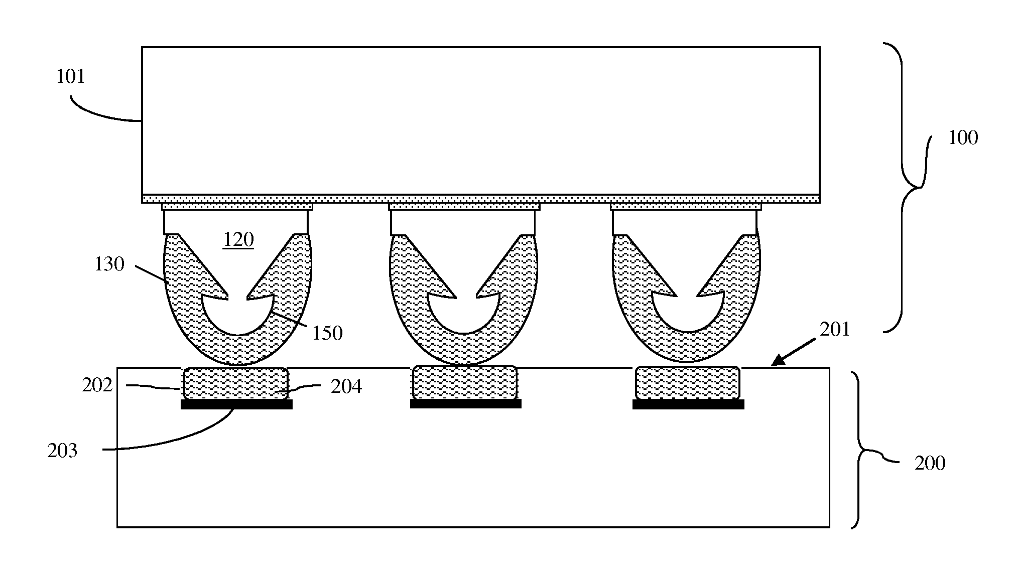
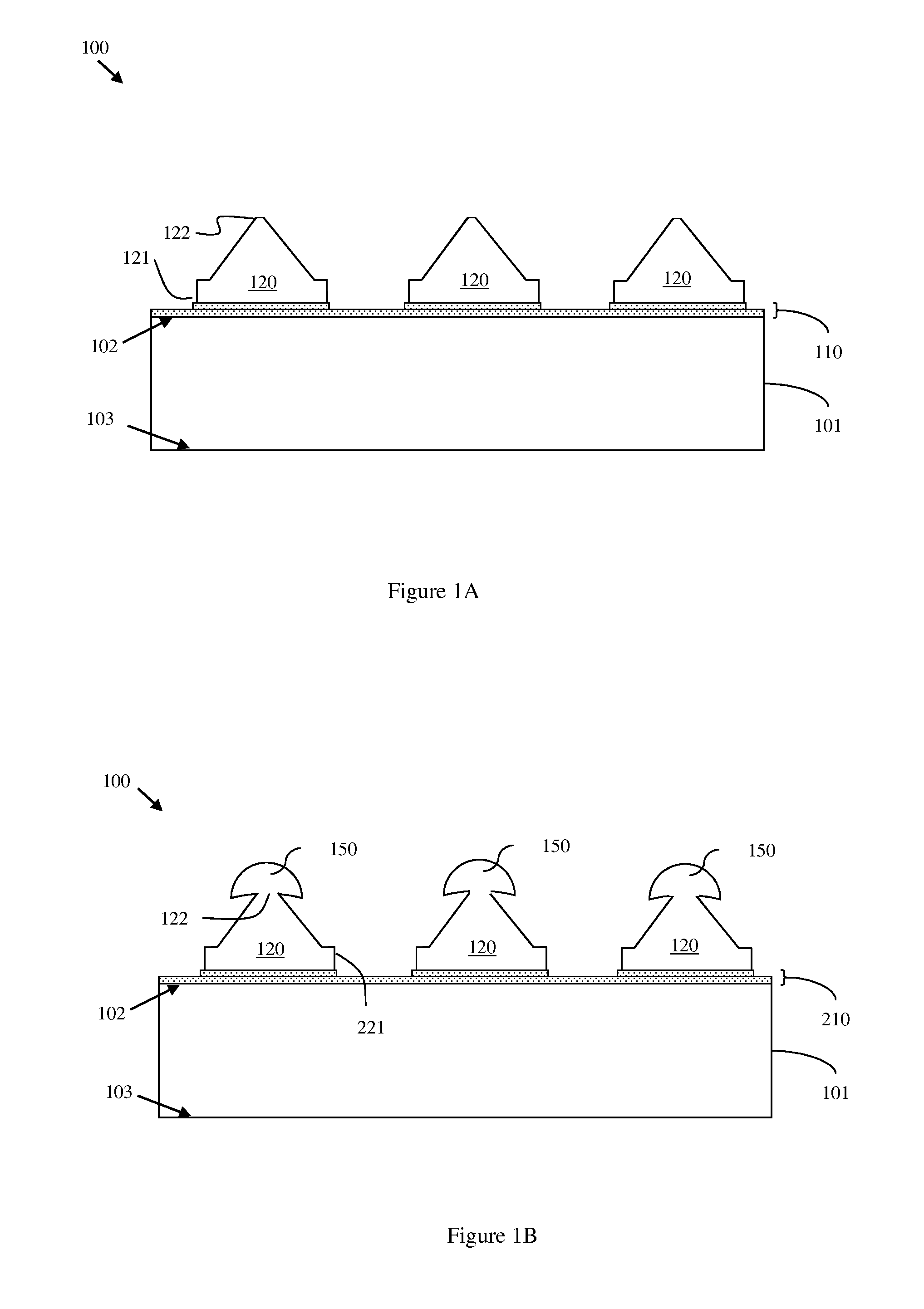
[0036]As mentioned above and discussed in detail in U.S. Patent Application Publication No. 2009 / 0146316 of Jadhav et al., filed on Dec. 5, 2007, published on Jun. 11, 2009, assigned to International Business Machines Corporation of Armonk, N.Y., and incorporated herein by reference, in a flip-chip assembly an inverted integrated circuit chip is typically mounted on a chip carrier by an array of controlled collapsed chip connections (i.e., C4 connections). The formation of such C4 connections usually involves the formation of solder balls on flat conductive pads on the active surface of an integrated circuit chip (e.g., on the same surface of the chip as the integrated circuit devices and, preferably, surrounding a core integr...


PUM


Abstract

Disclosed is a chip and method of forming the chip with improved conductive pads that allow for flexible C4 connections with a chip carrier or with another integrated circuit chip. The pads have a three-dimensional geometric shape (e.g., a pyramid or cone shape) with a base adjacent to the surface of the chip, a vertex opposite the base and, optionally, mushroom-shaped cap atop the vertex. Each pad can include a single layer of conductive material or multiple layers of conductive material (e.g., a wetting layer stacked above a non-wetting layer). The pads can be left exposed to allow for subsequent connection to corresponding solder bumps on a chip carrier or a second chip. Alternatively, solder balls can be positioned on the conductive pads to allow for subsequent connection to corresponding solder-paste filled openings on a chip carrier or a second chip.

Description

BACKGROUND[0001]1. Field of the Invention[0002]The embodiments generally relate to integrated circuit chips incorporated into electronic assemblies, such as flip-chip assemblies and stacked chip assemblies, using controlled collapsed chip connections (i.e., C4 connections). More particularly, the embodiments relate to an integrated circuit chip and a method of forming the chip with pyramid or cone-shaped conductive input / output (I / O) pads.[0003]2. Description of the Related Art[0004]As discussed in detail in U.S. Patent Application Publication No. 2009 / 0146316 of Jadhav et al., filed on Dec. 5, 2007, published on Jun. 11, 2009, assigned to International Business Machines Corporation of Armonk, N.Y., and incorporated herein by reference, in a flip-chip assembly an integrated circuit chip is typically mounted on a chip carrier by an array of controlled collapsed chip connections (i.e., C4 connections). The formation of such C4 connections usually involves the formation of solder balls...

Claims


Application Information

Patent Timeline
IPC IPC(8): H01L23/498H01L21/60
CPCH01L23/49816H01L2224/13019H01L24/13H01L24/81H01L2224/1147H01L2224/11901H01L2224/13144H01L2224/13147H01L2224/13155H01L2224/1357H01L2224/136H01L2224/13609H01L2224/13611H01L2224/13613H01L2224/13618H01L2224/1362H01L2224/13639H01L2224/13647H01L2224/81193H01L2224/81801H01L2924/01013H01L2924/01022H01L2924/01029H01L2924/0103H01L2924/01046H01L2924/01049H01L2924/01051H01L2924/01078H01L2924/01079H01L2924/01082H01L2924/14H01L2924/19041H01L24/11H01L2224/13018H01L2224/11902H01L2924/00013H01L2924/01005H01L2924/01024H01L2924/01033H01L2924/0105H01L2924/01074H01L2924/014H01L2224/1601H01L2224/81191H01L2924/00014H01L2924/01028H01L2224/13099H01L2924/00012H01L2224/02166H01L2224/10126H01L2224/13023H01L2224/13076H01L2224/16237H01L2924/351
Inventor DAUBENSPECK, TIMOTHY H.GAMBINO, JEFFREY P.MUZZY, CHRISTOPHER D.SAUTER, WOLFGANGSULLIVAN, TIMOTHY D.
Owner GLOBALFOUNDRIES INC
Features
  • Generate Ideas
  • Intellectual Property
  • Life Sciences
  • Materials
  • Tech Scout
  • Unparalleled Data Quality
  • Higher Quality Content
  • 60% Fewer Hallucinations
Learn More