Active element array substrate and flat display using the same
a technology of active elements and array substrates, applied in the field of array substrates, can solve problems such as damage to flat panel displays
- Summary
- Abstract
- Description
- Claims
- Application Information
AI Technical Summary
Benefits of technology
Problems solved by technology
Method used
Image
Examples
Embodiment Construction
[0022]It is to be understood that other embodiment may be utilized and structural changes may be made without departing from the scope of the present invention. Also, it is to be understood that the phraseology and terminology used herein are for the purpose of description and should not be regarded as limiting. The use of “including,”“comprising,” or “having” and variations thereof herein is meant to encompass the items listed thereafter and equivalents thereof as well as additional items. Unless limited otherwise, the terms “connected,”“coupled,” and “mounted,” and variations thereof herein are used broadly and encompass direct and indirect connections, couplings, and mountings.
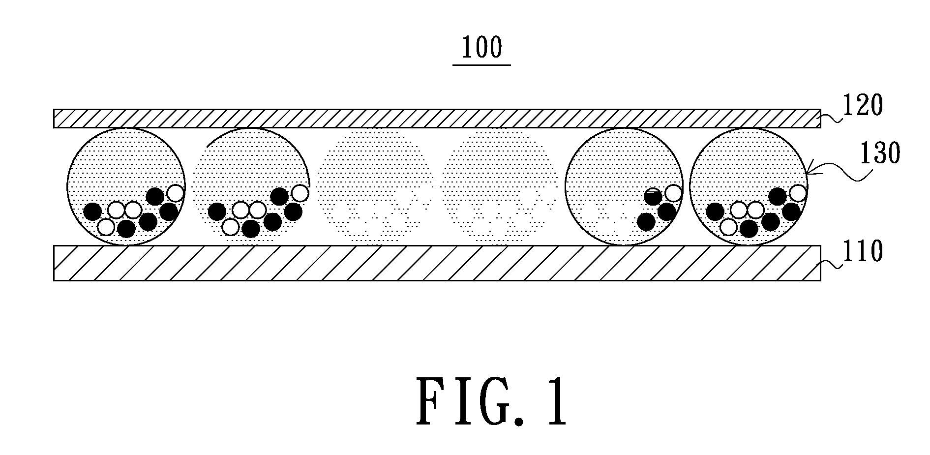
[0023]FIG. 1 is a schematic view of a flat panel display according to an embodiment of the present invention. In this embodiment, the electrophoretic display is illustrated as an example for description of the present invention. As known for ordinary skilled people in the art, the flat panel display may be ...
PUM
| Property | Measurement | Unit |
|---|---|---|
| weight percent | aaaaa | aaaaa |
| weight percent | aaaaa | aaaaa |
| weight percent | aaaaa | aaaaa |
Abstract
Description
Claims
Application Information


