Film deposition apparatus and method

a film deposition apparatus and film deposition technology, applied in chemical vapor deposition coating, metal material coating process, coating, etc., can solve the problems of difficult to completely remove silicon crystals 235, low product quality, and time-consuming process maintenance,

Inactive Publication Date: 2011-08-18
NUFLARE TECH INC
View PDF18 Cites 17 Cited by
  • Summary
  • Abstract
  • Description
  • Claims
  • Application Information

AI Technical Summary

Benefits of technology

[0033]The present invention relates to an apparatus and method used for film deposition. The apparatus comprising: a chamber; a gas inlet for supplying a deposition gas into the chamber; a gas outlet located at a bottom section of the chamber; a cylindrical liner for covering inner surfaces of the chamber, the liner including: a barrel section; a head section having an opening, the head section being smaller in horizontal cross-sectional area than the barrel section; and a stepped section for connecting the barrel section and the head section; a shower plate 20 which operates as a flow straightening vane, located at the opening of the head section of the liner, for producing a laminar flow of the deposition gas supplied into the chamber; a rotary shaft located at a bottom section of the chamber and extending upwardly into the barrel section of the liner; a rotary drum connected to an upper end of the rotary shaft; and a susceptor assembly on which to place a substrate, the susceptor assembly being supported by the rotary drum inside the barrel section, wherein the susceptor assembly includes: a susceptor on which to place the substrate, the susceptor being supported by the rotary drum; support posts attached to the susceptor; and a ring plate ...

Problems solved by technology

The silicon crystals 235 obstructing the liner 202 can be removed by, for example, hydrofluoric acid cleaning, but the complete removal of the silicon crystals 235 is not easy.
Those dust particles may contaminate films to be deposited on substrates during subsequent vapor-phase epitaxial processes and can be a factor that lowers product qua...

Method used


Image

  • Film deposition apparatus and method
  • Film deposition apparatus and method
  • Film deposition apparatus and method

Examples


Embodiment Construction

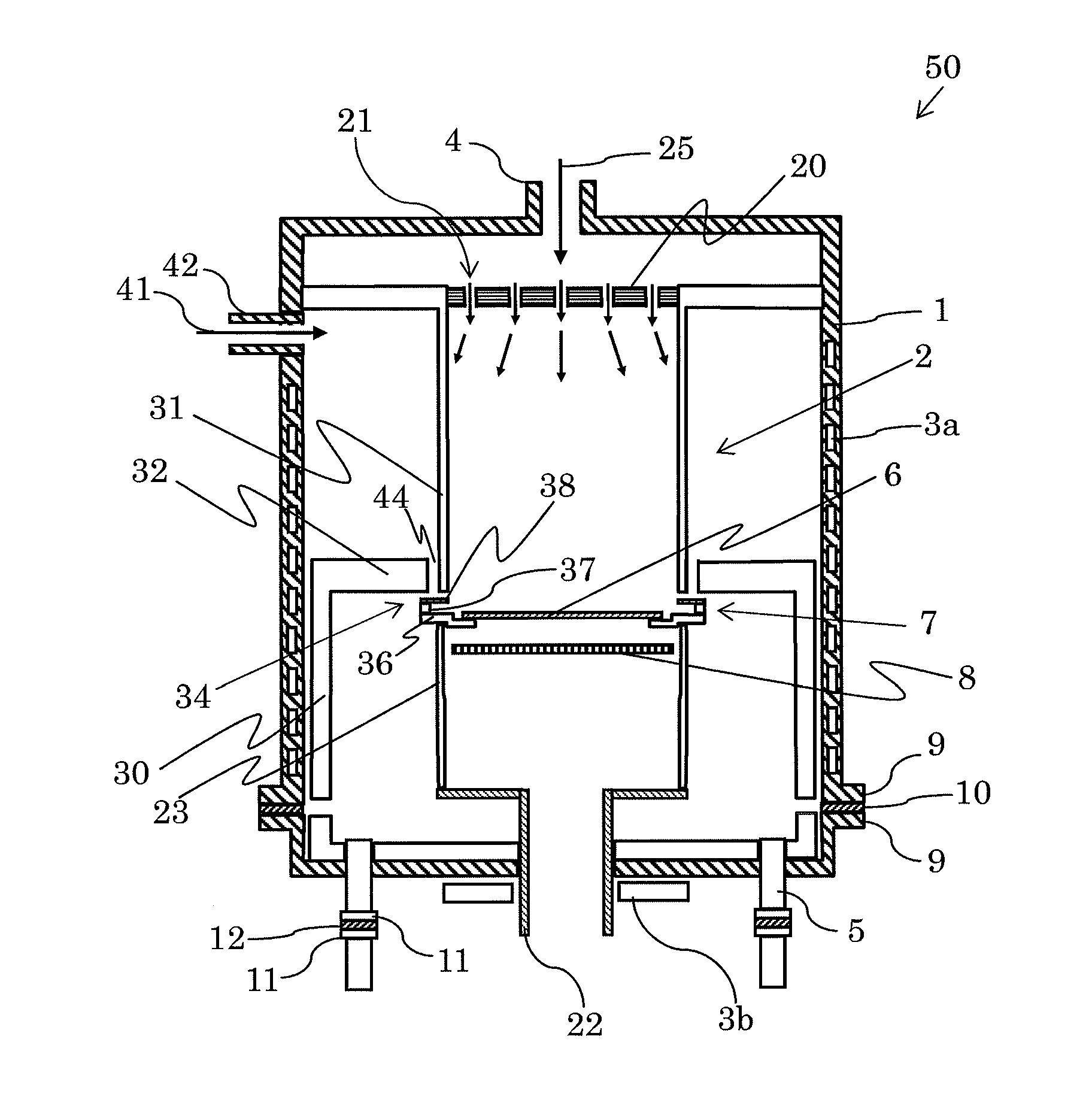
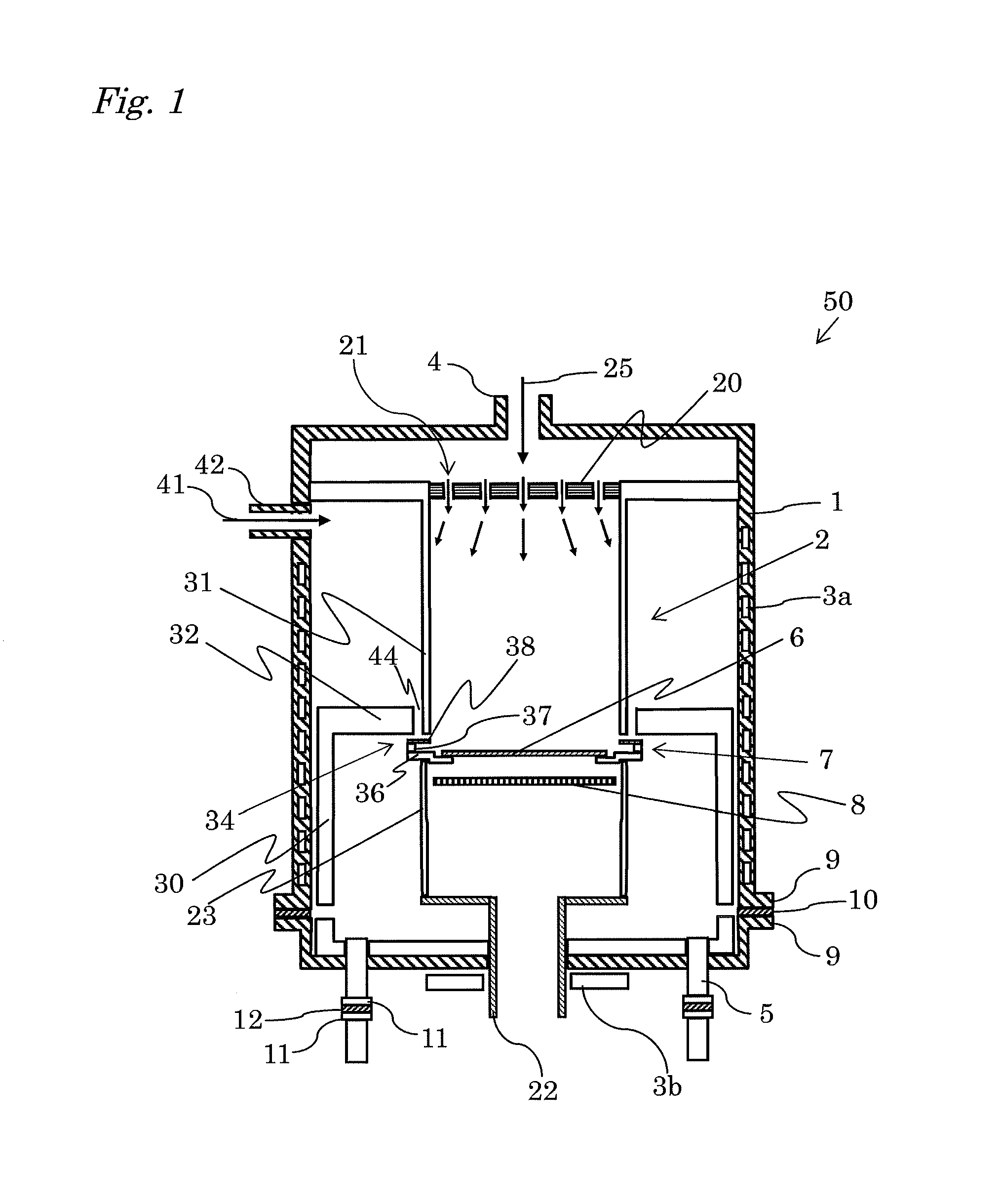
[0039]FIG. 1 is a cross sectional diagram illustrating a deposition apparatus according to an embodiment of the present invention.

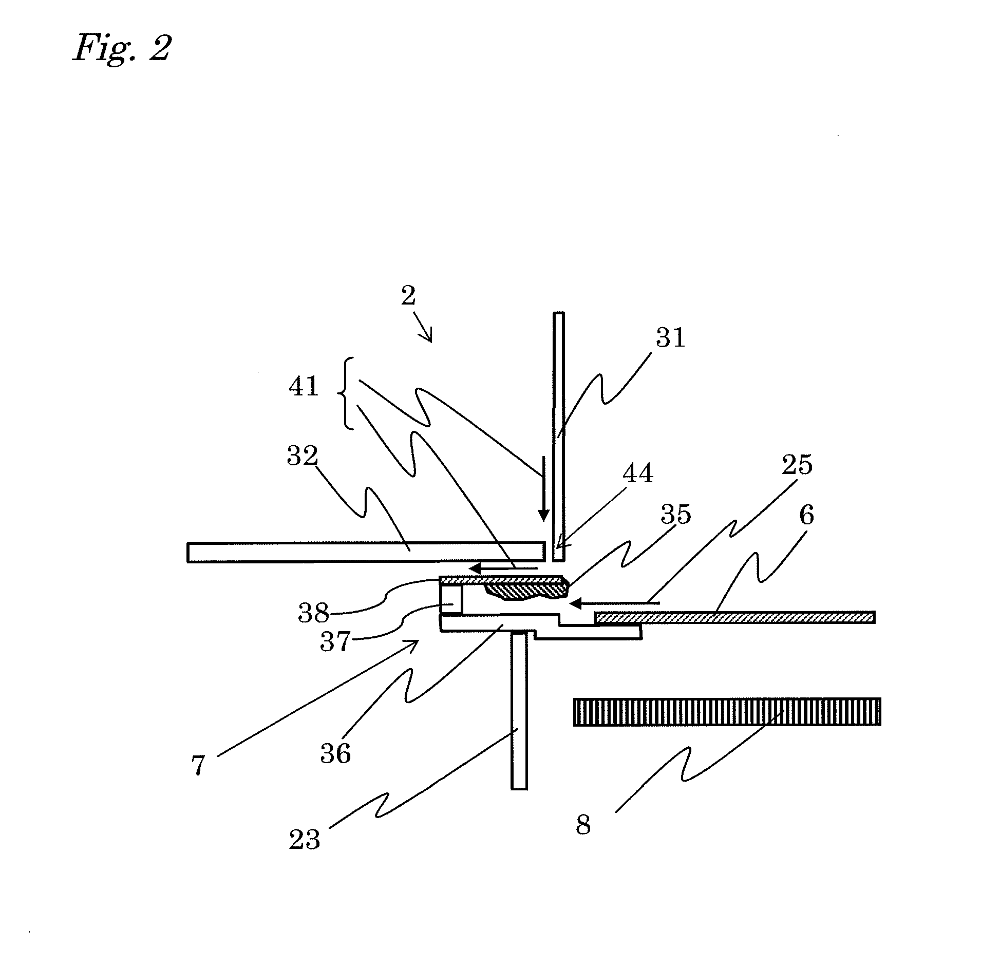
[0040]The deposition apparatus 50 of FIG. 1 comprises of the following components: a film deposition chamber 1 having upper and lower sections; a hollow, cylindrical liner 2 located inside the chamber 1 to protect its inner walls; coolant passageways 3a and 3b through which coolant, for example, water flows to cool the chamber 1; a gas inlet 4 from which to introduce a deposition gas 25; gas outlets 5 from which to discharge the deposition gas 25 after use; a susceptor assembly 7 on which to place a semiconductor substrate 6 such as a silicon wafer or the like; a heater 8, fixed to a support (not illustrated) for heating the substrate 6; flanges 9 for connecting the upper and lower sections of the chamber 1; a packing material 10 for sealing the flanges 9; flanges 11 used for connection of the gas outlets 5 to pipes; and packing material 12 for sealing th...


PUM

PropertyMeasurementUnit
Areaaaaaaaaaaa
Semiconductor propertiesaaaaaaaaaa

Abstract

A chamber includes at its upper section a gas inlet from which to introduce a deposition gas. The inner walls of the chamber are covered by a cylindrical liner, and the chamber houses a susceptor assembly on which to place a semiconductor substrate. The liner includes a barrel section inside which the susceptor assembly is placed; a head section that is located right below the gas inlet and smaller in horizontal cross-sectional area than the barrel section; and a stepped section that connects the barrel section and the head section. The susceptor assembly is formed by fixing a ring plate to a susceptor via support posts. The ring plate covers the periphery of the stepped section of the liner. By the deposition gas flowing in a downward direction from the gas inlet into the chamber, a crystalline film is formed on the substrate positioned on the susceptor assembly.

Description

BACKGROUND OF THE INVENTION[0001]1. Field of the Invention[0002]The present invention relates to a film deposition apparatus and a film deposition method.[0003]2. Background Art[0004]Epitaxy or epitaxial growth is often employed in manufacturing such semiconductor devices that require relatively thick crystalline films. Examples of these devices include power semiconductor devices such as insulated-gate bipolar transistors (IGBTs) and the like.[0005]Vapor-phase epitaxy, a form of epitaxial growth, requires that the film deposition chamber in which a semiconductor substrate (e.g., a silicon wafer) has been placed be kept at atmospheric pressure (0.1 MPa or 760 Torr) or lower if silicon (Si) crystals are to be grown on the substrate to obtain an Si monocrystalline substrate.[0006]After the substrate has been heated to a given temperature, the chamber is supplied with a deposition gas, which is typically formed by mixing a silicon source gas with a boron-based dopant gas (e.g., diboran...

Claims


Application Information

Patent Timeline
IPC IPC(8): C23C16/458C23C16/455C23C16/46
CPCC23C16/4402C23C16/4585C23C16/455
Inventor SUZUKI, KUNIHIKOYAJIMA, MASAYOSHI
Owner NUFLARE TECH INC
Why Eureka
Try Eureka