Crenulated wiring structure and method for integrated circuit interconnects

Inactive Publication Date: 2011-09-22
IBM CORP
View PDF12 Cites 11 Cited by
  • Summary
  • Abstract
  • Description
  • Claims
  • Application Information

AI Technical Summary

Problems solved by technology

The resistance increase with decreasing pitch as technology shrinks causes many issues.
In addition, it becomes more difficult to fill higher aspect ratio t

Method used


Image

  • Crenulated wiring structure and method for integrated circuit interconnects
  • Crenulated wiring structure and method for integrated circuit interconnects
  • Crenulated wiring structure and method for integrated circuit interconnects

Examples


Embodiment Construction

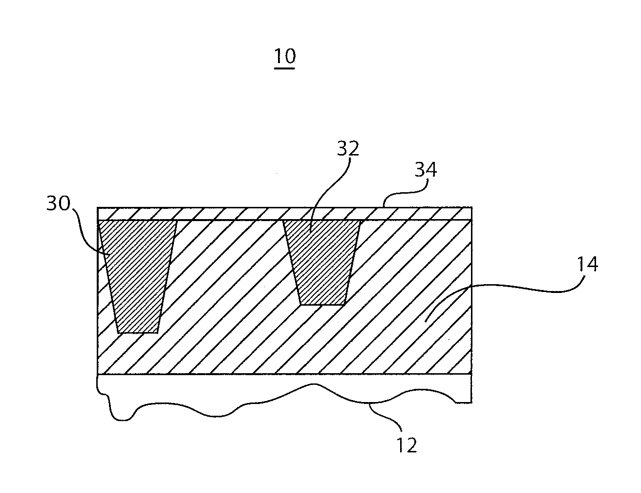
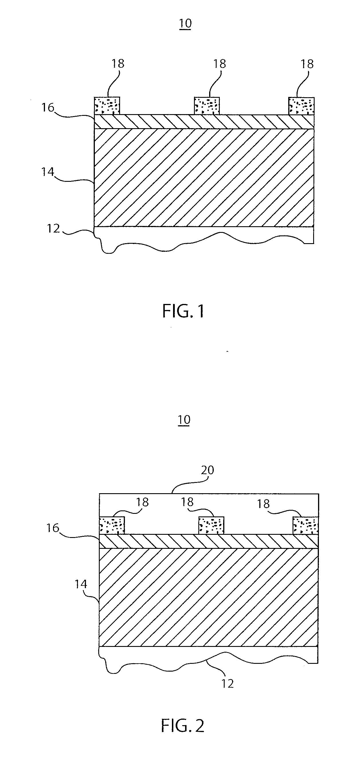
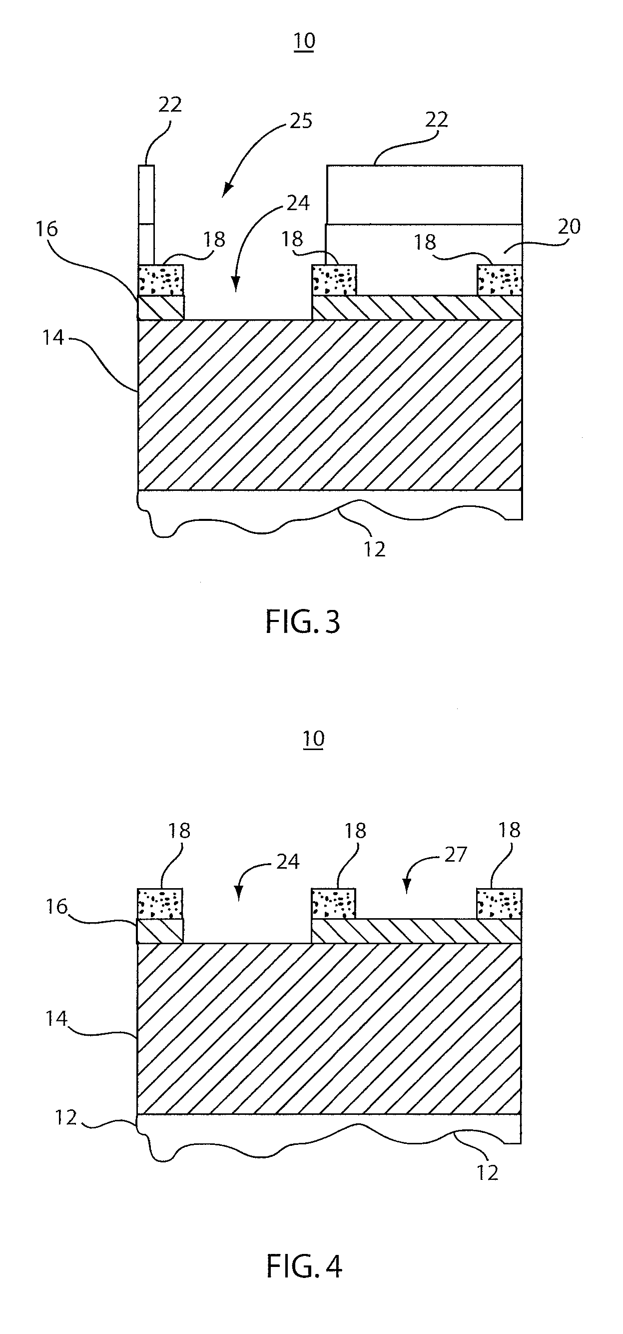
[0023]In accordance with the present principles, space available in a via level dielectric is employed to add or extend wiring in a regular, periodic fashion. Instead of increasing aspect ratio (AR), a depth of a wire conductor is periodically increased along a line or trench. This increase is staggered such that it is not adjacent to an increased depth portion of an adjacent line. Rather, the increased depths are staggered between adjacent lines. One advantage includes that the overall resistance of the line decreases without adding a significant amount of capacitance. Other advantages include, e.g., larger metal grains are possible in the increased depth regions, and electro-migration (EM) lifetimes are improved.

[0024]It is to be understood that the present invention will be described in terms of a given illustrative architecture having particular materials of fabrication and structures; however, other architectures, structures, substrate materials and process features and steps m...


PUM


Abstract

A method for forming crenulated conductors and a device having crenulated conductors includes forming a hardmask layer on a dielectric layer, and patterning the hardmask layer. Trenches are etched in the dielectric layer using the hardmask layer such that the trenches have shallower portions and deeper portions alternating along a length of the trench. A conductor is deposited in the trenches such that crenulated conductive lines are formed having different depths periodically disposed along the length of the conductive line.

Description

BACKGROUND[0001]1. Technical Field[0002]The present invention relates to wiring structures and methods for making the same, and more particularly to crenulated wiring to improve performance of integrated circuits in view of shrinking technology sizes.[0003]2. Description of the Related Art[0004]As technology shrinks, resistive-capacitive (RC) impedance associated with back end of line (BEOL) wiring increases dramatically. Such wiring, often referred to as “thin-wires”, is mostly driven by the fact that resistance (as well as the resistivity) increases with decreasing dimensions. The resistance increase with decreasing pitch as technology shrinks causes many issues.[0005]One way to attempt to control these issues is to increase the aspect ratio (AR) of the wires or increase volume of the conductors, both of which have severe drawbacks. In the first case, increasing AR increases capacitance. In addition, it becomes more difficult to fill higher aspect ratio trenches. Increasing conduc...

Claims


Application Information

Patent Timeline
IPC IPC(8): H01L23/528H01L21/768
CPCH01L21/31144H01L21/76804H01L21/76816H01L23/5283H01L2924/0002H01L2924/3011H01L2924/00
Inventor BONILLA, GRISELDAHUANG, ELBERT E.NITTA, SATYANARAYANA V.PONOTH, SHOM
Owner IBM CORP
Why Eureka
Try Eureka