Imaging device

a technology of a device and an image, applied in the field of imaging devices, can solve the problems of shading correction, bias shading among plural viewpoint images, etc., and achieve the effect of preventing bias shading

Inactive Publication Date: 2011-09-29
FUJIFILM CORP
View PDF34 Cites 24 Cited by
  • Summary
  • Abstract
  • Description
  • Claims
  • Application Information

AI Technical Summary

Benefits of technology

[0023]For example, a 3D image (stereoscopic image) including a left-viewpoint image and a right-viewpoint image by both the horizontal photography and the vertical photography can be generated, and the biased shading can be prevented.
[0024]Moreover, the photographing optical system may include a zoom lens, and the shading correction part may change the amount of shading correction depending on the zoom position of the zoom lens. That is to say, it ...

Problems solved by technology

However, in the above-mentioned imaging devices, there is a problem of biased shading among plural viewpoint images in a pupil splitting direction.
Even in an imaging device employing a single photographing optical system, since the shading result from the chro...

Method used


Image

  • Imaging device
  • Imaging device
  • Imaging device

Examples


first embodiment

[0064]First of all, a first embodiment will be described.

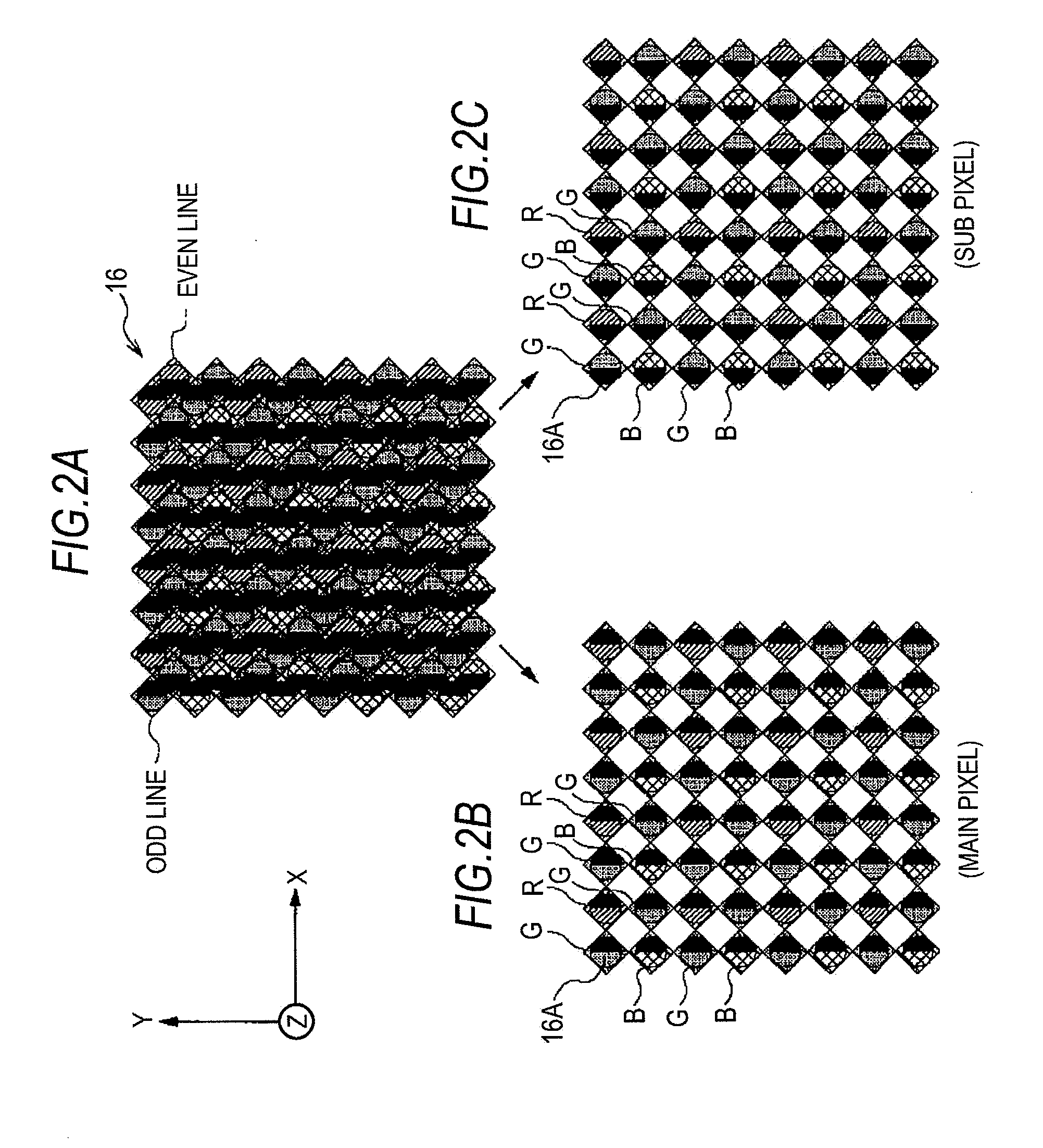
[0065]FIGS. 2A to 2C are diagrams partially illustrating the configuration of the CCD 16. FIG. 2A illustrating a main pixel group and a sub-pixel group arranged in a honeycomb alignment, FIG. 2B illustrates only the main pixel group, and FIG. 2C illustrates only the sub-pixel group.

[0066]As shown in FIGS. 2A to 2C, the CCD 16 includes main pixels (hereinafter, also referred to as “A-face pixel”) of odd lines in the vertical direction (Y-axis direction in the drawings) and sub-pixels (hereinafter, also referred to as “B-face pixels”) of even lines in the vertical direction, which all arranged in a matrix shape, and independently reads out pixel signals photo-electrically converted by the main pixel group and the sub-pixel group as main-viewpoint images (A-face images) and sub-viewpoint images (B-face images).

[0067]As shown in FIGS. 2A to 2C, out of the pixels having color filters of R (red), G (green) and B (blue), horizontal l...

second embodiment

[0119]the present invention (where plural pupil splitting directions exist) will be described below.

[0120]FIG. 9A shows an arrangement of main pixels+sub-pixels, FIG. 9B shows an arrangement of only the main pixels, and FIG. 9C shows an arrangement of only the sub-pixels.

[0121]The CCD 16 in this embodiment includes plural pixel group pairs (pixel group sets) corresponding to plural pupil splitting directions (the X direction and the Y direction in the drawings). Specifically, the CCD 16 includes a first pixel group pair 61 including a first main pixel group 61a and a first sub-pixel group 61b corresponding to a first pupil splitting direction (the X direction in the drawings) and a second pixel group pair 62 including a second main pixel group 62a and a second sub-pixel group 62b corresponding to a second pupil splitting direction (the Y direction in the drawings).

[0122]The imaging device 10 according to this embodiment acquires the left viewpoint image and the right viewpoint image...

third embodiment

[0125]the present invention (where the phase-difference shading amount of a pixel is physically adjusted) will be described below.

[0126]FIG. 10 is a diagram schematically illustrating a part of the CCD 16 in this embodiment.

[0127]As shown in FIG. 10, in the central part R1 of the light-receiving surface, the light-blocking area of the light-blocking member 16Aa for the main pixel PDca (photo diodes of the main pixel group) and the light-blocking area of the light-blocking member 16Ab for the sub-pixel PDcb (photo diodes of the sub-pixel group) are equal to each other. That is to say, the aperture area of the aperture 16Ba for the main pixel PDca and the aperture area of the aperture 16Bb for the sub-pixel PDcb are equal to each other. In the peripheral parts R2 and R3 in the pupil splitting direction (X direction) of the light-receiving surface, the light-blocking area of the light-blocking member 16Aa for the main pixel PDma and the light-blocking area of the light-blocking member ...


PUM


Abstract

An imaging device comprising a single photographing optical system, an image sensor having a plurality of pixels for obtaining a plurality of viewpoint images by photo-electrically converting a luminous flux passing through different regions of the photographing optical system, and a shading correction part for conducting a shading correction to the plurality of viewpoint images. The shading correction part varies the amount of shading correction based on light-reduction property for one viewpoint image among the plurality of viewpoint images with respect to the amount of shading correction based on light-reduction property for the other viewpoint image among the plurality of viewpoint images.

Description

BACKGROUND OF THE INVENTION[0001]1. Field of the Invention[0002]The present invention relates to a technique of obtaining plural viewpoint images by photo-electrically converting a luminous flux passing through different regions of a single photographing optical system.[0003]2. Description of the Related Art[0004]Conventionally, an imaging device having an optical system as shown in FIG. 16 has been known (JP2009-527007A).[0005]In FIG. 16, a luminous flux passing through different regions in a left-right direction (vertical or crosswise direction in the drawing) of a main lens 1 and a relay lens 2 is split by a mirror 4, and the split luminous fluxes are photo-electrically converted by image sensors 7 and 8 via focus lenses 5 and 6.[0006]FIGS. 17A to 17C are diagrams illustrating a difference in an object image focused on an image sensor due to a difference in an object distance (distant and close). Note that, in FIGS. 17A to 17C, the mirror 4 shown in FIG. 16 is abbreviated to comp...

Claims


Application Information

Patent Timeline
IPC IPC(8): H04N9/64
CPCH04N5/3572H04N23/672H04N23/673H04N25/61H04N25/611
Inventor ENDO, HIROSHI
Owner FUJIFILM CORP
Why Eureka
Try Eureka