Structure and method to integrate embedded dram with finfet

a technology of embedded dram and finfet, which is applied in the field of semiconductors, can solve the problems of difficult integration of finfets with planar logic, compromising memory cell functionality, and wreaking the effects of worsening these tradeoffs

Active Publication Date: 2011-10-13
IBM CORP
View PDF10 Cites 65 Cited by
  • Summary
  • Abstract
  • Description
  • Claims
  • Application Information

AI Technical Summary

Problems solved by technology

The use of eDRAM as microprocessor cache, however, involves making tradeoffs between performance parameters, such as speed, retention time and power consumption, and production parameters, such as yield and design complexity.
Due to their small sizes, memory cells are especially susceptible to process-induced variations, which worsen these tradeoffs and compromise memory cell functionality.
However, the integration of FinFETs with planar logic is difficult due to vertical topography, especially since DRAM processes generally rely on bulk silicon wafer substrates.
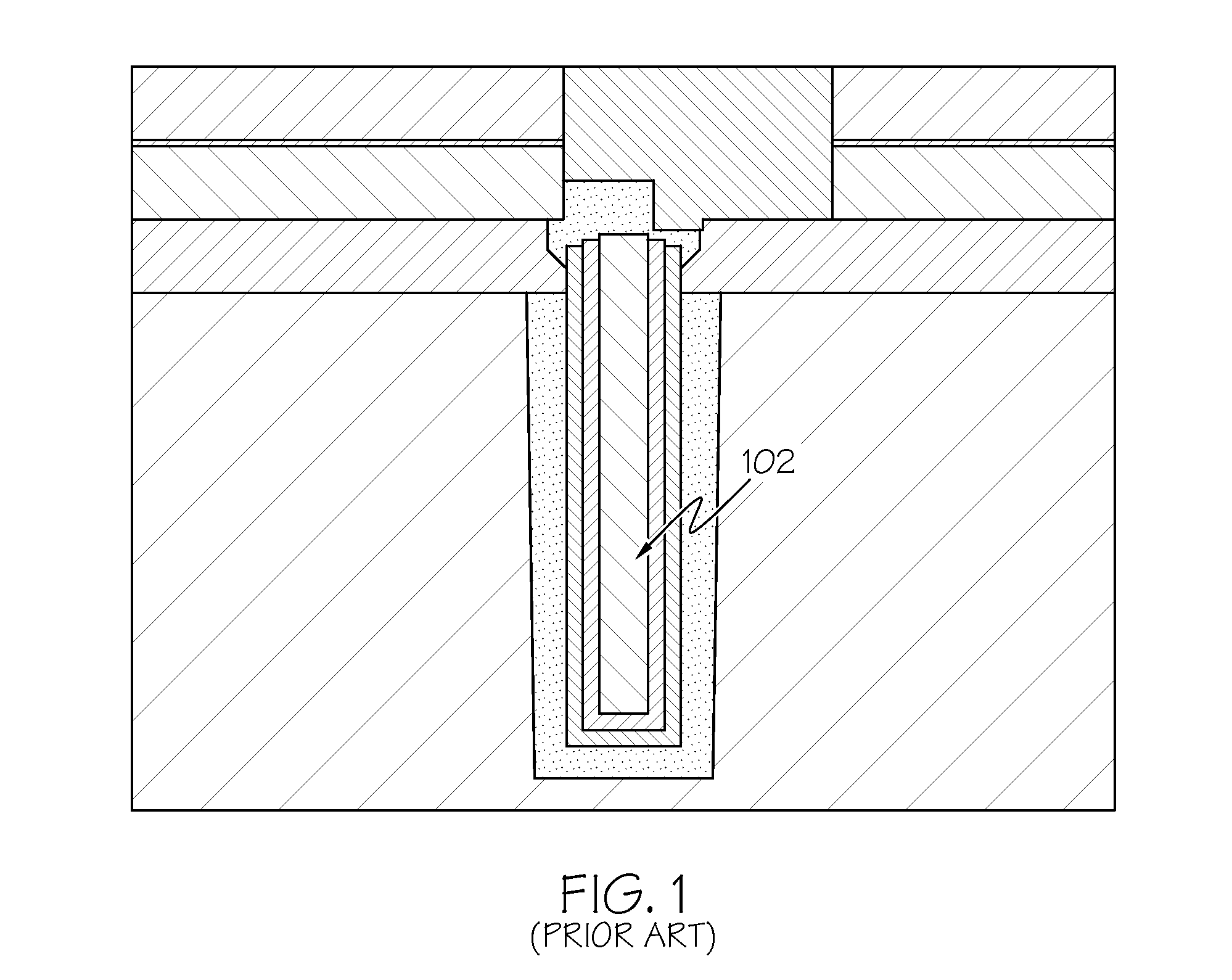
Various problems in extrapolating planar DRAM technology to FinFETs lie in the fact that there is no unprocessed side to the body of the transistor where the capacitor can be strapped to.
As such, conventional techniques are unable to use FinFETs for eDRAM.

Method used


Image

  • Structure and method to integrate embedded dram with finfet
  • Structure and method to integrate embedded dram with finfet
  • Structure and method to integrate embedded dram with finfet

Examples


Embodiment Construction

[0012]As required, detailed embodiments of the present invention are disclosed herein; however, it is to be understood that the disclosed embodiments are merely exemplary of the invention, which can be embodied in various forms. Therefore, specific structural and functional details disclosed herein are not to be interpreted as limiting, but merely as a basis for the claims and as a representative basis for teaching one skilled in the art to variously employ the present invention in virtually any appropriately detailed structure. Further, the terms and phrases used herein are not intended to be limiting; but rather, to provide an understandable description of the invention.

[0013]The terms “a” or “an”, as used herein, are defined as one as or more than one. The term plurality, as used herein, is defined as two as or more than two. Plural and singular terms are the same unless expressly stated otherwise. The term another, as used herein, is defined as at least a second or more. The ter...


PUM


Abstract

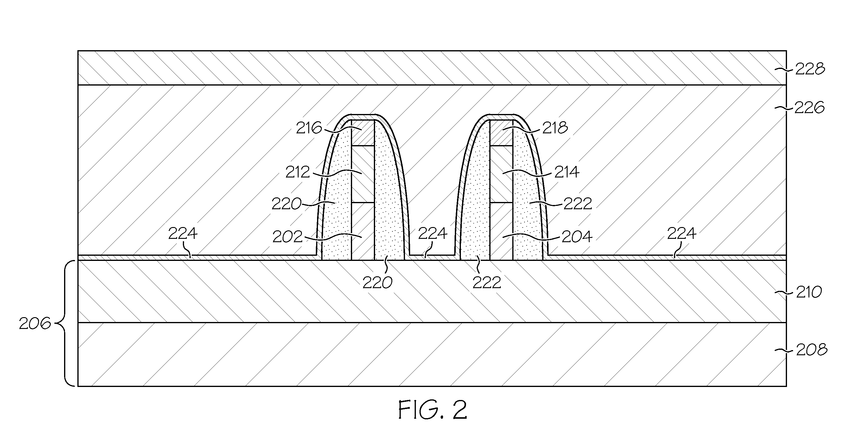
A transistor includes a first fin structure and at least a second fin structure formed on a substrate. A deep trench area is formed between the first and second fin structures. The deep trench area extends through an insulator layer of the substrate and a semiconductor layer of the substrate. A high-k metal gate is formed within the deep trench area. A polysilicon layer is formed within the deep trench area adjacent to the metal layer. The polysilicon layer and the high-k metal layer are recessed below a top surface of the insulator layer. A poly strap in the deep trench area is formed on top of the high-k metal gate and the polysilicon material. The poly strap is dimensioned to be below a top surface of the first and second fin structures. The first fin structure and the second fin structure are electrically coupled to the poly strap.

Description

FIELD OF THE INVENTION[0001]The present invention generally relates to the field of semiconductors, and more particularly relates to embedding DRAM with FinFETs.BACKGROUND OF THE INVENTION[0002]It is a common practice to integrate memory and logic functions on a common semiconductor substrate. In such a configuration, when the memory function is performed by a dynamic random access memory (DRAM) cell, the circuitry is referred to as embedded DRAM (eDRAM).[0003]The use of eDRAM as microprocessor cache, however, involves making tradeoffs between performance parameters, such as speed, retention time and power consumption, and production parameters, such as yield and design complexity. Due to their small sizes, memory cells are especially susceptible to process-induced variations, which worsen these tradeoffs and compromise memory cell functionality. Thus, steps need to be taken to minimize process-induced variations.[0004]The use of undoped channel devices such as fin-field effect tran...

Claims


Application Information

Patent Timeline
Patent Type & Authority Applications(United States)
IPC IPC(8): H01L27/108H01L21/28
CPCH01L21/26586H01L21/845H01L27/1211H01L27/10879H01L27/10891H01L27/10826H10B12/36H10B12/056H10B12/488
Inventor KANAKASABAPATHY, SIVANANDAJAGANNATHAN, HEMANTHWANG, GENG
Owner IBM CORP
Why Eureka
Try Eureka