Test device

a technology for testing devices and semiconductor devices, which is applied in the direction of solid-state devices, instruments, material analysis, etc., can solve the problems of small components, difficult detection of shear forces, and difficult to solve small components, so as to improve the absolute breaking load and repeatability. , the effect of good results

Inactive Publication Date: 2011-11-10
NORDSON CORP
View PDF11 Cites 0 Cited by
  • Summary
  • Abstract
  • Description
  • Claims
  • Application Information

AI Technical Summary

Benefits of technology

[0013]Such a tool element may be arranged to pre-load the crystal so as to improve stability thereof.
[0015]In a preferred embodiment the interface between the support element and the crystal, and / or between the crystal and the shield comprises a force distributing layer which is adapted to give substantially uniform planar contact. Such a layer may for example comprise an epoxy resin which is spread whilst fluid onto the respective interface surfaces, and cures after assembly of the apparatus to ensure that planar contact occurs. In this way point and line loads can be avoided.
[0016]The layer need only be very thin, and sufficient only to accommodate any misalignment which may be present. A particular advantage of epoxy resin is that the adjacent components are also retained in one another adhesively, so that the apparatus becomes unitary.

Problems solved by technology

Difficulties arise because of the very small dimensions of the components, the precision with which the testing device must be positioned, and the very small forces and deflections which are to be measured.
In the case of impact testing, where the tool is moving at high velocity before contact with the ball deposit, shear forces are not easy to detect.

Method used


Image

  • Test device
  • Test device
  • Test device

Examples


first embodiment

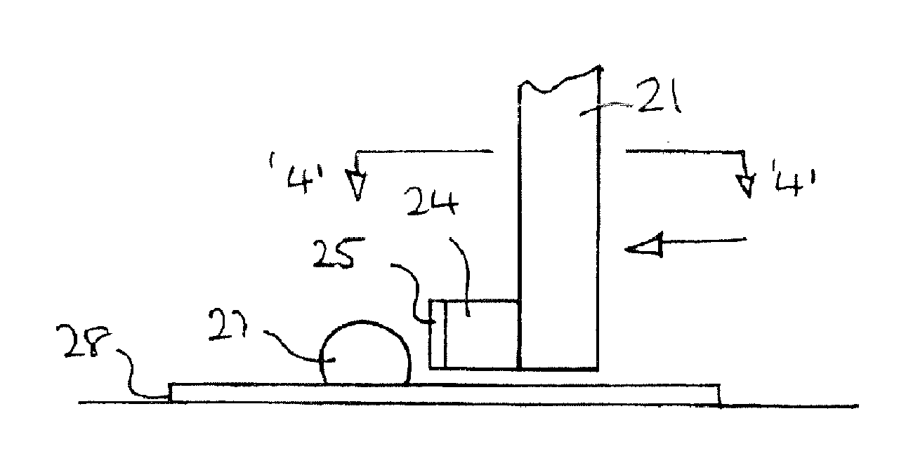
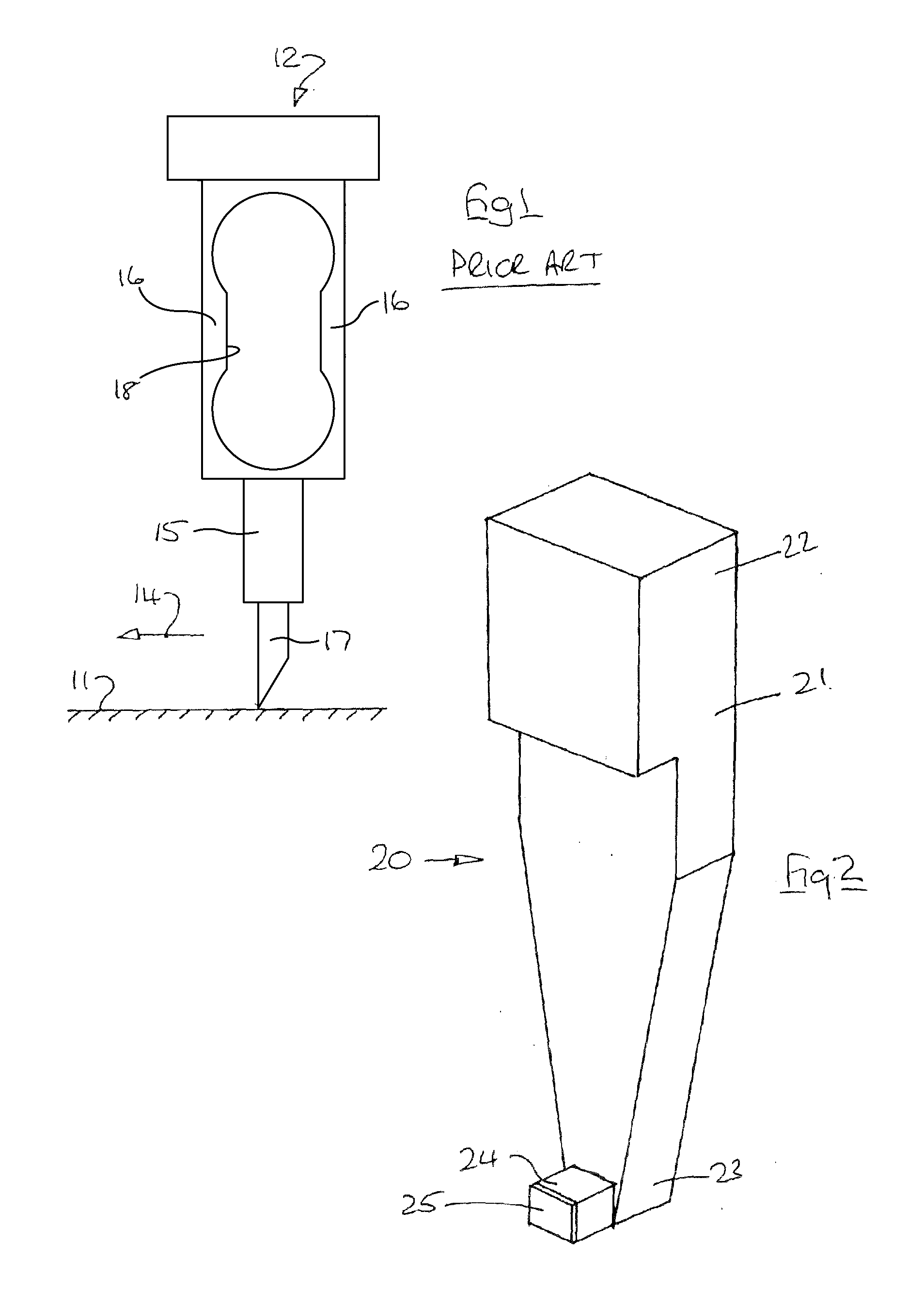
[0035]FIG. 2 shows the invention, and illustrates a tool 20 comprising a support element 21, the upper end 22 of which is adapted for direct connection to a prior art test head 12, or to a cartridge thereof in any suitable manner. The latter arrangement ensures interchangeability of components for existing test apparatus.

[0036]The lower end 23 tapers and has a piezo-electric crystal 24 attached thereto. The outer face of the crystal has a shield 25. The crystal is illustrated as a cube, but other shapes are of course possible, such as a cylinder.

[0037]The crystal has a width generally of the same order as the ball deposit to be tested, for example 100 μm. Not illustrated are the usual electrical connections of the crystal whereby changing stress of the crystal can be detected, and by calibration, calculation of the actual load.

[0038]The shield can be any suitable material covering adapted to protect the crystal from mechanical damage yet allow loads to be fully transmitted thereto. ...

second embodiment

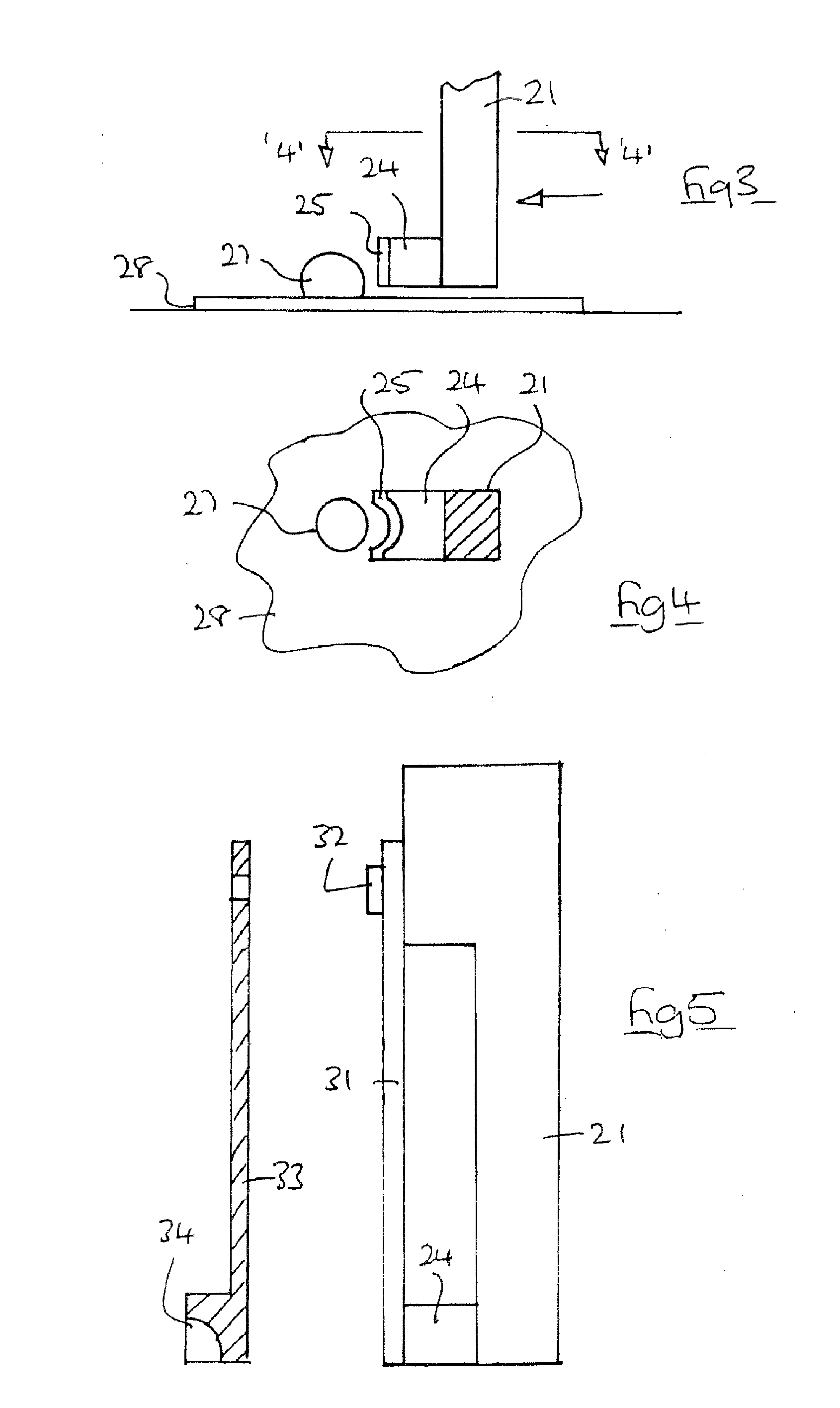
[0041]A second embodiment is illustrated in FIG. 5 and comprises the support element 21 from which an anvil 31 is suspended on a pin 32 or clip of any suitable kind. The tool is plate-like and can directly apply a compressive load to the crystal 24. In a preferred embodiment the tool is biased against the crystal by internal resilience thereof, for example by reducing the thickness of the portion in contact with the upper end 22.

[0042]An alternative anvil 33 is illustrated in section, and has a part spherical recess 34 to closely engage the ball deposit.

[0043]FIG. 6 illustrates an alternative embodiment in which the undersurface of a tool 40 has an upward rake 49 so that the height of the leading edge 46 above the substrate 48 can be accurately determined prior to shear test. The rake may be any suitable angle (typically in the range)15-30° which ensures clearance behind the leading edge whilst maintaining mechanical integrity of the tool.

[0044]FIG. 7 corresponds to FIG. 5, and show...


PUM

PropertyMeasurementUnit
diameteraaaaaaaaaa
heightaaaaaaaaaa
thicknessaaaaaaaaaa

Abstract

Shear test apparatus for gold and solder balls of a semiconductor substrate comprises a support element (21) on which is provided a piezo-electric crystal (24) in the direct shear load path. The crystal (24) may have a shield (25). The interface between shield and crystal, and crystal and support element may include an epoxy resin layer to distribute force and retain the components as a unit.

Description

CROSS-REFERENCE TO RELATED APPLICATIONS[0001]This application is a continuation of application Ser. No. 12 / 764,191, filed Apr. 21, 2010, which is a continuation of application Ser. No. 11 / 573,005, filed Sep. 11, 2008 and now U.S. Pat. No. 7,730,790, which is the National Stage of International Application No. PCT / GB2005 / 003105, filed Aug. 5, 2005, which claims priority to Great Britain Application No. 0417773.9, filed Aug. 10, 2004 and Great Britain Application No. 0513896.1, filed Jul. 6, 2005. The content of each of these applications is hereby incorporated by reference herein in its entirety.BACKGROUND[0002]This invention concerns a device for testing the shear strength of a bond in a semiconductor device, and more particularly the strength of a bond between a substrate and a means of electrical connection thereto, typically a part-spherical deposit of solder or gold.[0003]Semiconductor devices are very small, typically from 0.2 mm square to 25 mm square. These devices have sites...

Claims


Application Information

Patent Timeline
Patent Type & Authority Applications(United States)
IPC IPC(8): G01N3/24
CPCG01N3/24G01N2203/021G01N2203/0051G01N3/42H01L2224/859
Inventor SYKES, ROBERT JOHN
Owner NORDSON CORP
Why Eureka
Try Eureka