
Chip unit and stack package having the same

a technology of stack package and chip unit, which is applied in the direction of electrical apparatus, semiconductor device details, semiconductor/solid-state device devices, etc., can solve the problems of difficult to form a semiconductor package, the semiconductor chip is likely to warp or break, and the bonding cannot be properly implemented using conductive wires, so as to minimize the occurrence of warpage and fail.

Active Publication Date: 2011-11-10
SK HYNIX INC
View PDF15 Cites 44 Cited by
  • Summary
  • Abstract
  • Description
  • Claims
  • Application Information

AI Technical Summary

Benefits of technology

[0007]Embodiments of the present invention are directed to a chip unit which can minimize the occurrence of warpage and fails such as cracks in a semiconductor chip and a stack package having the same.

Problems solved by technology

In this regard, as the thickness of the semiconductor chip decreases and an overhang increases, problems are caused in that bouncing occurs and bonding cannot be properly implemented using conductive wires.
When implementing bonding by using conductive wires, that is, attaching conductive wires to a thin semiconductor chip ess, the semiconductor chip is likely to warp or break owing to its small thickness.
In addition, due to the decrease in the thickness of the semiconductor chip, failures such as cracks may result in the semiconductor chip during a semiconductor chip out process or a semiconductor chip pickup process for attaching the semiconductor chip.
As a consequence, not only is it difficult to form a semiconductor package using the semiconductor chip with the small thickness, but the productivity of the semiconductor package also markedly decreases.

Method used


Image

  • Chip unit and stack package having the same
  • Chip unit and stack package having the same
  • Chip unit and stack package having the same

Examples


Embodiment Construction

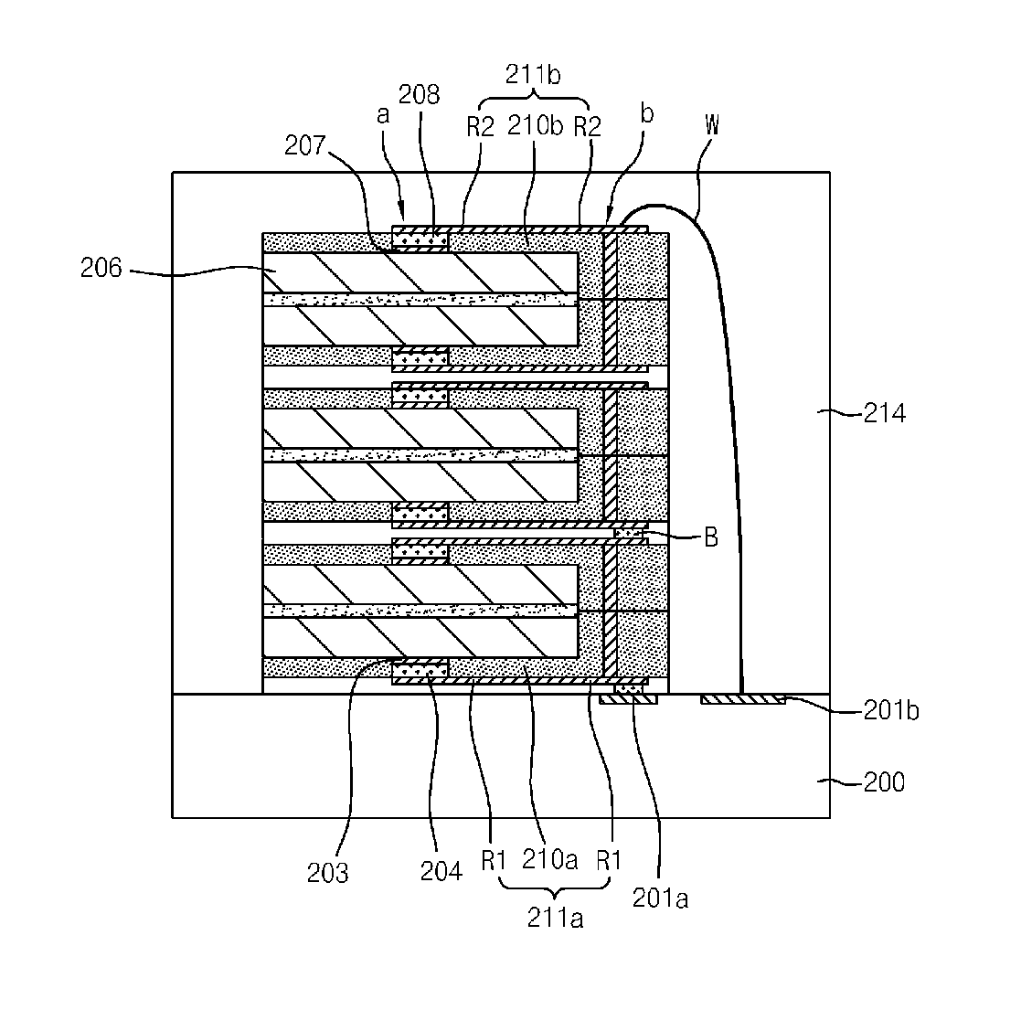
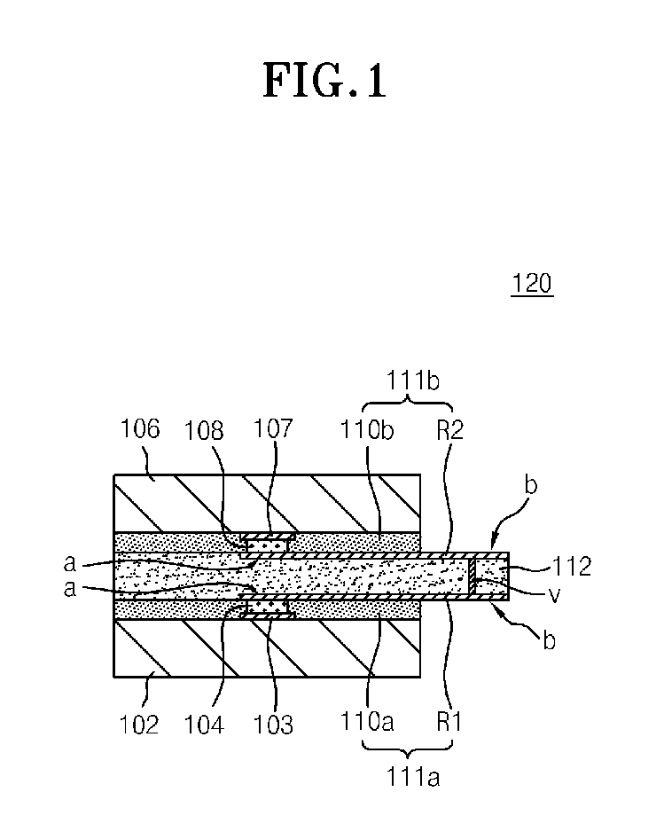
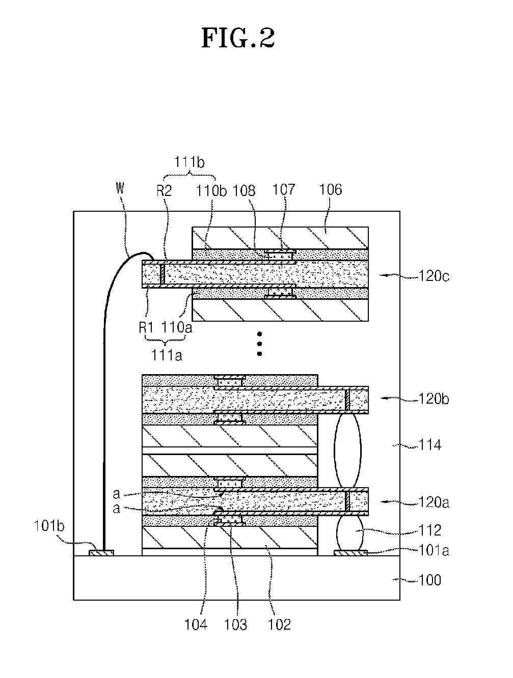
[0027]According to an embodiment of the present invention, after preparing two semiconductor chips with center type pads, the two semiconductor chips are placed to face each other in such a manner that their center type pads define, for example, mirror image symmetry with respect to each other, and a resultant structure is molded using a flexible material such as an RCC (resin coated copper foil) and a resin containing a metallic material, as a result of which a chip unit is formed.

[0028]By forming the chip unit in this way, since the center type pads of the two semiconductor chips are electrically connected with each other, the two semiconductor chips can function as one driving chip unit.

[0029]As a consequence, in an embodiment of the present invention, as the chip unit is formed as described above, it is possible to form a stack package with a high capacity and a small thickness.

[0030]Further, in an embodiment of the present invention, when forming the chip unit, since the soft p...


PUM


Abstract

A chip unit includes: a first semiconductor chip and a second semiconductor chip disposed such that their surfaces for forming first bonding pads and second bonding pads face each other; first and second connection members disposed on the surfaces of the first and second semiconductor chips for forming the first and second bonding pads, and having redistribution lines which have one ends connected with the first and second bonding pads and the other ends projecting beyond one edges of the first and second semiconductor chips and films; an adhesive member interposed between the first connection members and the second connection members; and via patterns passing through the adhesive member and connecting projecting portions of the redistribution lines of the first and second connection members with each other.

Description

CROSS-REFERENCE TO RELATED APPLICATIONS[0001]The present application claims priority to Korean patent application number 10-2010-0042453 filed on May 6, 2010, which is incorporated herein by reference in its entirety.TECHNICAL FIELD[0002]The present invention relates to a chip unit and a stack package having the same, and more particularly, to a chip unit which can minimize the occurrence of warpage and failures such as cracks in a semiconductor chip, and a stack package having the same.BACKGROUND OF THE INVENTION[0003]Recently, as semiconductors are used in most electronic products with the development of the electronic industry, various sized and shaped semiconductor packages are used. Specifically, in small-sized electronic appliances and mobile products, semiconductor chips, which have a high processing speed, light weight and highly integrated, are increasingly used. Thus, semiconductor packages with appropriate sizes and shapes are used in these products.[0004]Meanwhile, in or...

Claims


Application Information

Patent Timeline
Patent Type & Authority Applications(United States)
IPC IPC(8): H01L23/28
CPCH01L24/32H01L24/48H01L2225/1035H01L24/29H01L24/16H01L25/0657H01L25/105H01L2224/13022H01L2224/48091H01L2224/48147H01L2224/48227H01L2225/06517H01L2225/0652H01L2225/06524H01L2225/06527H01L2225/06548H01L2225/06558H01L2225/06562H01L2225/06572H01L2225/1052H01L2225/1058H01L2924/19107H01L2924/3511H01L23/3121H01L23/5389H01L23/562H01L24/05H01L24/13H01L2924/00014H01L2924/3512H01L2924/00H01L2224/0401H01L2224/16225H01L2924/181H01L2924/00012H01L2224/45099H01L2224/45015H01L2924/207H01L23/12H01L23/48
Inventor LEE, KYU WONJOH, CHEOL HODO, EUN HYEKIM, JI EUNSHIN, HEE MIN
Owner SK HYNIX INC
Features
  • Generate Ideas
  • Intellectual Property
  • Life Sciences
  • Materials
  • Tech Scout
  • Unparalleled Data Quality
  • Higher Quality Content
  • 60% Fewer Hallucinations
Learn More