Systems and methods for detecting design and process defects on a wafer, reviewing defects on a wafer, selecting one or more features within a design for use as process monitoring features, or some combination thereof

a technology of design and process defects and system and method, which is applied in the direction of semiconductor/solid-state device testing/measurement, image enhancement, instruments, etc., can solve the problems of affecting the electrical parameters of the device, the operation of semiconductor manufacturing processes closer to the limitations of process performance capability, and the need to detect defects of decreasing siz

Active Publication Date: 2011-11-10
KLA TENCOR TECH CORP
View PDF13 Cites 176 Cited by
  • Summary
  • Abstract
  • Description
  • Claims
  • Application Information

AI Technical Summary

Benefits of technology

[0018]A further embodiment relates to a computer-implemented method for selecting one or more features within a design for use as process monitoring features. The method includes simulating how features in a design will print on a wafer at different values of one or more parameters of a lithography process. The different values include nominal values corresponding to a center of a process window of the lithography process. The method a

Problems solved by technology

However, as the dimensions of semiconductor devices decrease, inspection becomes even more important to the successful manufacture of acceptable semiconductor devices because smaller defects can cause the devices to fail.
For instance, as the dimensions of semiconductor devices decrease, detection of defects of decreasing size has become necessary since even relatively small defects may cause unwanted aberrations in the semiconductor devices.
As design rules shrink, however, semiconductor manufacturing processes may be operating closer to the limitations on the performance capability of the processes.
In addition, smaller defects can have an impact on the electrical parameters of

Method used


Image

  • Systems and methods for detecting design and process defects on a wafer, reviewing defects on a wafer, selecting one or more features within a design for use as process monitoring features, or some combination thereof
  • Systems and methods for detecting design and process defects on a wafer, reviewing defects on a wafer, selecting one or more features within a design for use as process monitoring features, or some combination thereof
  • Systems and methods for detecting design and process defects on a wafer, reviewing defects on a wafer, selecting one or more features within a design for use as process monitoring features, or some combination thereof

Examples


Embodiment Construction

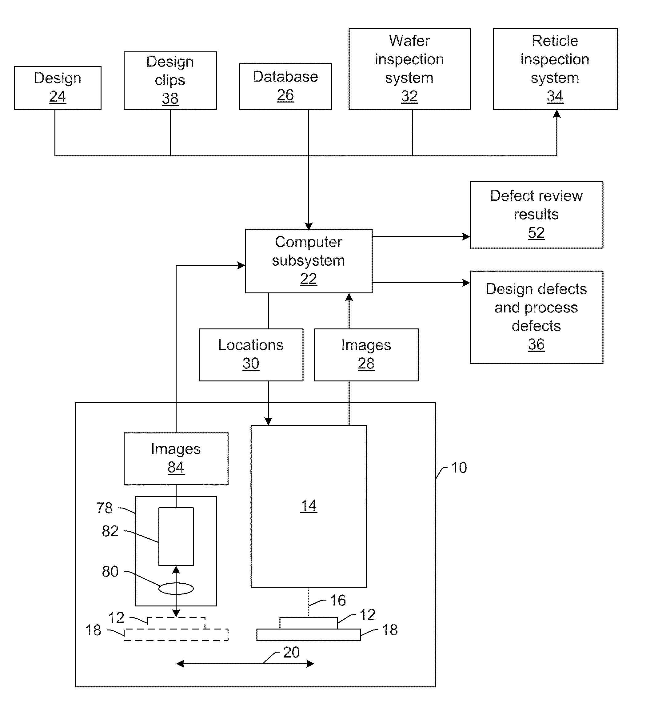
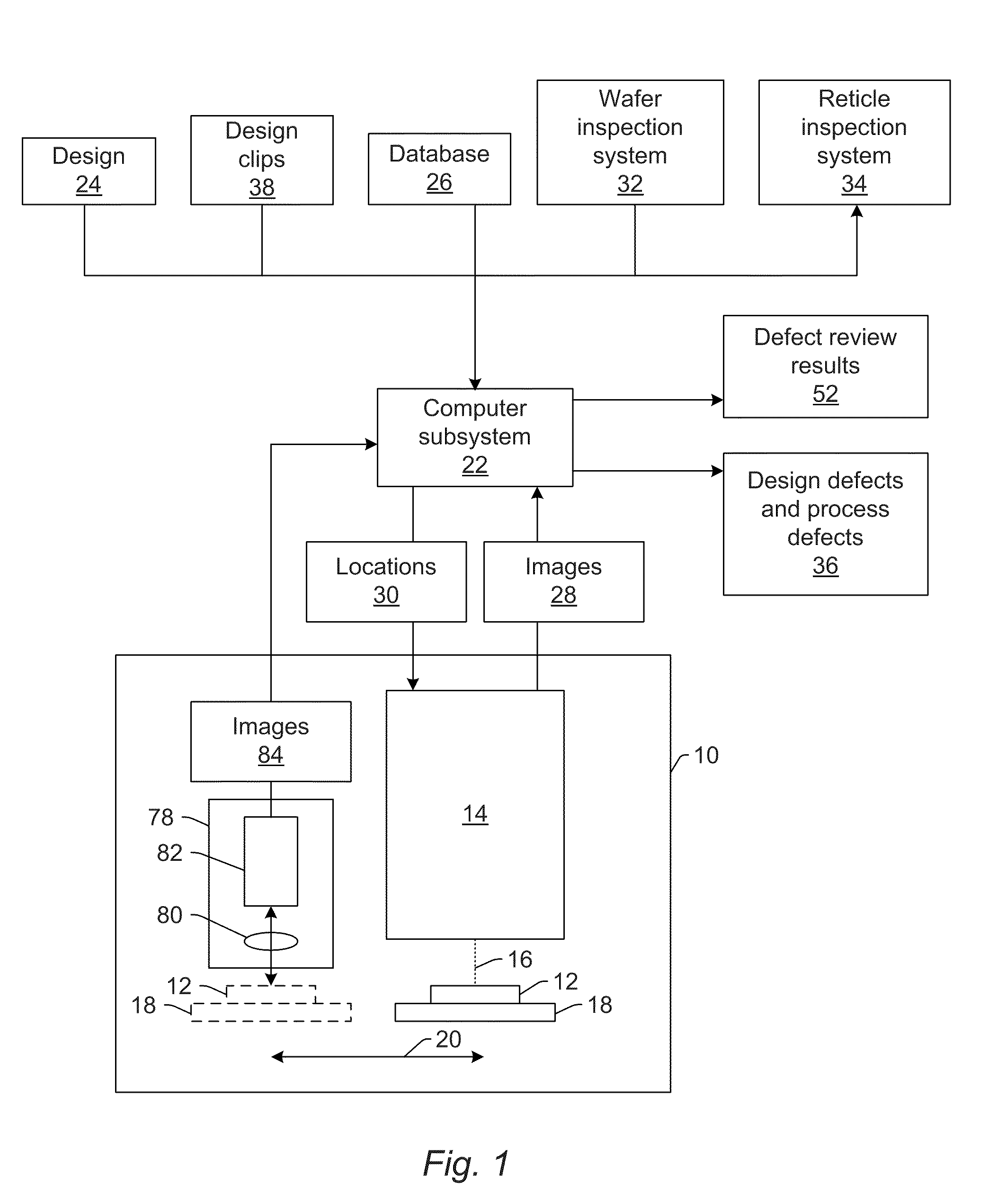
[0026]The term “design” as used herein generally refers to the physical design (layout) of an IC and data derived from the physical design through complex simulation or simple geometric and Boolean operations. The design may include not only layout information, but electrical and material design information as well. Basically, the design may include any design information that is used in the creation of a “device.” In addition, an image of a reticle acquired by a reticle inspection system and / or derivatives thereof can be used as a “proxy” or “proxies” for the design. Such a reticle image or a derivative thereof can serve as a substitute for the design layout in any embodiments described herein that use a design. The design may include any other design data or design data proxies described in commonly owned U.S. patent application Ser. No. 11 / 561,735 by Kulkarni et al., published as U.S. Patent Application Publication No. 2007 / 0156379 on Jul. 5, 2007, and Ser. No. 11 / 561,659 by Zafa...


PUM


Abstract

Various systems and methods for detecting design and process defects on a wafer, reviewing defects on a wafer, selecting one or more features within a design for use as process monitoring features, or some combination thereof are provided.

Description

CROSS-REFERENCE TO RELATED APPLICATIONS[0001]This application is a National Stage application of International Application No. PCT / US09 / 46379 filed Jun. 5, 2009, which claims priority to U.S. Provisional Application No. 61 / 060,554 entitled “Systems and Methods for Detecting Design and Process Defects on a Wafer, Reviewing Defects on a Wafer, Selecting One or More Features Within a Design for Use as Process Monitoring Features, or Some Combination Thereof,” filed Jun. 11, 2008, which is incorporated by reference as if fully set forth herein.BACKGROUND OF THE INVENTION[0002]1. Field of the Invention[0003]The present invention generally relates to systems and methods for detecting design and process defects on a wafer, reviewing defects on a wafer, selecting one or more features within a design for use as process monitoring features, or some combination thereof.[0004]2. Description of the Related Art[0005]The following description and examples are not admitted to be prior art by virtue...

Claims


Application Information

Patent Timeline
IPC IPC(8): G06F17/50
CPCG01N21/956G06T7/0006G06T2207/10061G06T2207/30148H01L2924/0002H01L22/12H01L2924/00G03F7/705G06F30/398
Inventor FOUQUET, CHRISTOPHESAIDIN, ZAINEDELSTEIN, SERGIONANJANGUD, SAVITHAHESS, CARL
Owner KLA TENCOR TECH CORP
Why Eureka
Try Eureka