
Liquid crystal display device and inspection method thereof

a display device and liquid crystal technology, applied in measurement devices, electrical testing, instruments, etc., can solve the problems of inability to detect fan-out parts between data pads and data lines, data transistors not formed at data integrated circuits,

Active Publication Date: 2011-11-17
SAMSUNG DISPLAY CO LTD
View PDF4 Cites 12 Cited by
  • Summary
  • Abstract
  • Description
  • Claims
  • Application Information

AI Technical Summary

Benefits of technology

[0011]The embodiment is to provide a liquid crystal display device and inspection method thereof that are capable of detecting malfunctions of connection lines regardless of downsizing of data integrated circuits.
[0022]According to the liquid crystal display device and the inspection method thereof, there is a advantage that the liquid crystal display device is able to detect malfunctions of connection lines by using of the first data transistors that is configured to be overlapped with a data integrated circuit, and is able to detect malfunctions of liquid crystal cells by using of the second data transistors that is configured at an outer area to be un-overlapped with the data integrated circuit. Here, the first data transistors are able to be configured with a possible minimum size due to detecting only malfunctions of connection lines, and thus are able to be disposed to be overlapped with a data circuit.

Problems solved by technology

In this case, there is a disadvantage that the data transistors are not formed at the data integrated circuits, which are gradually downsized, and the overlapped area of the panel.
However, in the event that the data transistors are directly connected to the data lines, there is a disadvantage that malfunctions of connection lines (i.e., fan-out part) between data pads and data lines is not detected.

Method used


Image

  • Liquid crystal display device and inspection method thereof
  • Liquid crystal display device and inspection method thereof
  • Liquid crystal display device and inspection method thereof

Examples


Embodiment Construction

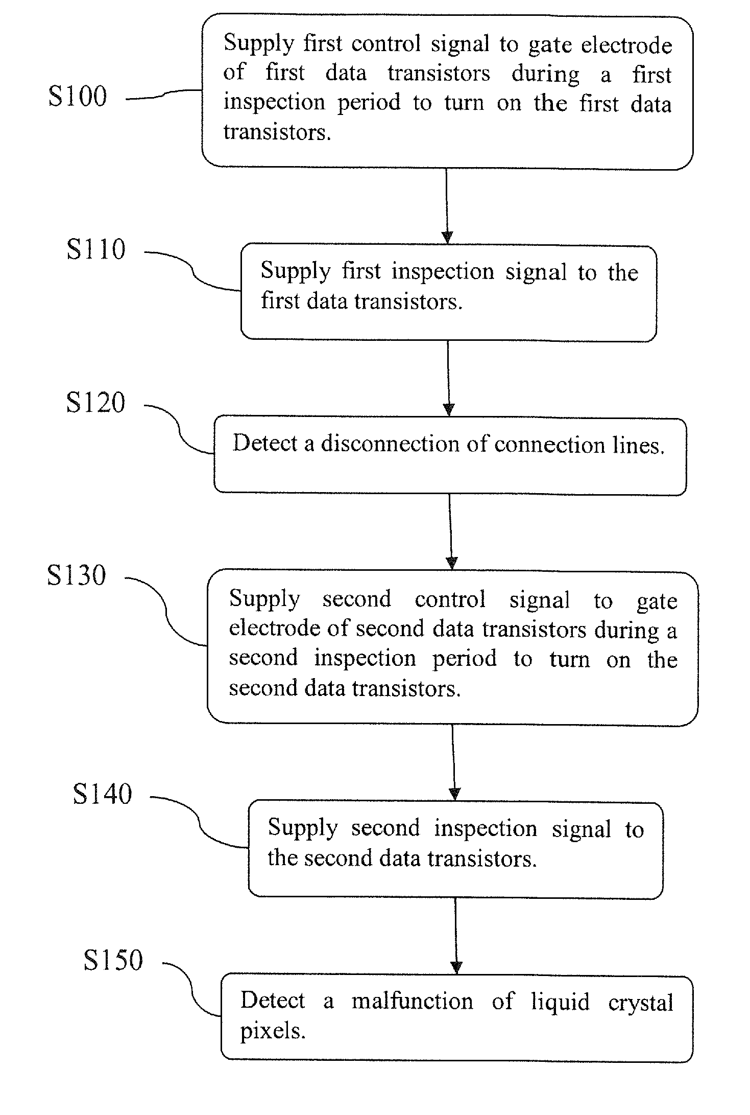
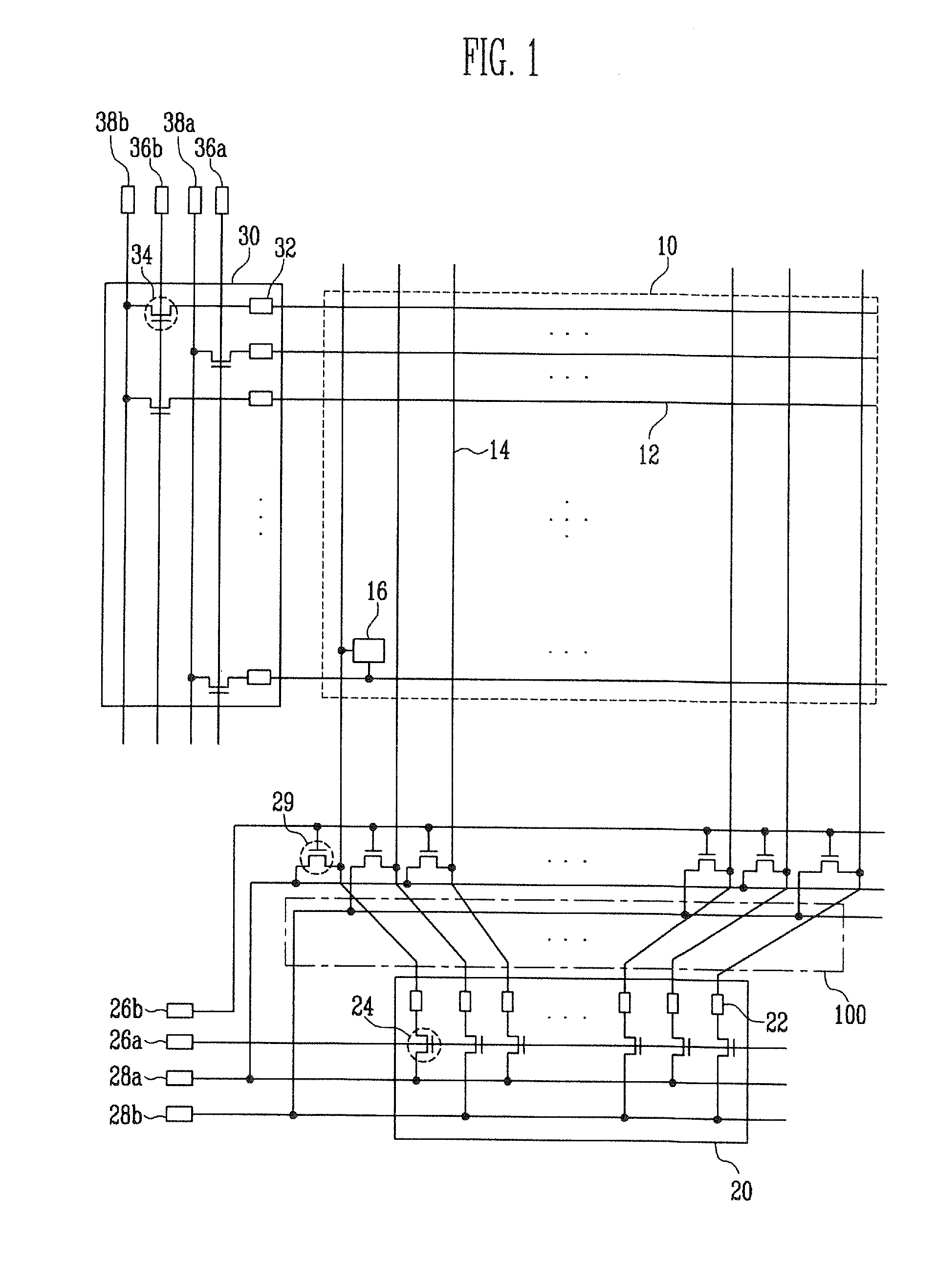
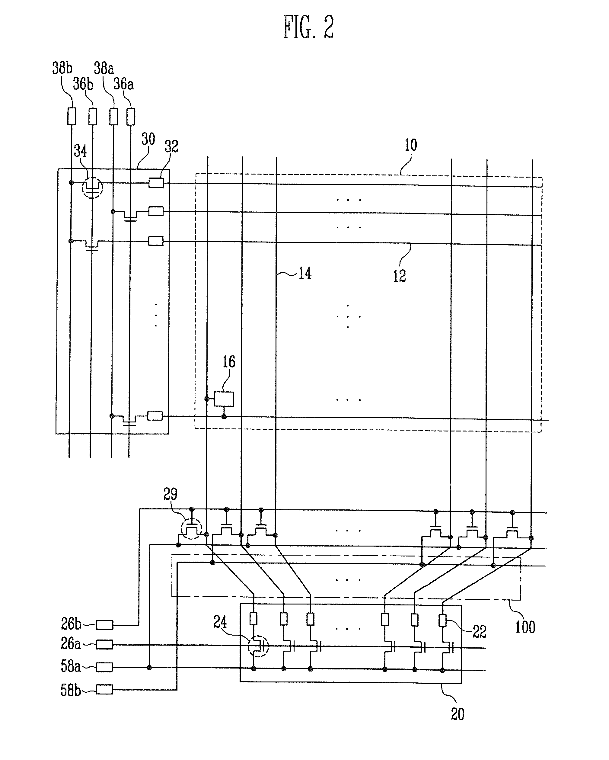
[0028]The liquid crystal display (LCD) device displays images by controlling light transmittance ratio of liquid crystal cells disposed in the form of matrix on a liquid crystal panel according to data signals. To achieve this, the liquid crystal display device includes a liquid crystal panel having liquid crystal cells and a drive circuit to drive the liquid crystal cells. The LCD panel includes an upper substrate and a lower substrate. The upper substrate includes a red color filter, a green color filter and a blue color filter, and a black matrix formed between the color filters. A common electrode is formed on the color filters. The lower substrate includes thin film transistors (TFT) formed at each of the liquid crystal cells, pixel electrodes formed to be connected to the TFT, and wire electrodes formed to be connected to the TFT. The liquid crystal panel is produced through a processing procedure, and goes through an inspection process to detect short and open of scan lines a...


PUM


Abstract

The embodiment is to provide a liquid crystal display device capable of detecting malfunctions. The liquid crystal display device includes pixels configured to be connected to scan lines and data lines, data pads electrically connected to the data lines, a data integrated circuit supplying data signals to the data lines through the data pads, first data transistors coupled to the data pads, and second data transistors coupled to the data lines. The first data transistors are disposed on the data integrated circuit and the second data transistors are separated from the data integrated circuit.

Description

CLAIM OF PRIORITY[0001]This application makes reference to, incorporates the same herein, and claims all benefits accruing under 35 U.S.C. §119 from an application earlier filed in the Korean Intellectual Property Office on 13 May 2010 and there duly assigned Serial No. 10-2010-0044905.BACKGROUND OF THE INVENTION[0002]1. Field of the Invention[0003]The embodiment relates to a liquid crystal display device and an inspection method thereof, and more particularly, to a liquid crystal display device and an inspection method thereof that are capable of detecting malfunctions.[0004]2. Description of the Related Art[0005]The liquid crystal display (LCD) device displays images by controlling light transmittance ratio of liquid crystal cells disposed in the form of matrix on a liquid crystal panel according to data signals. To achieve this, the liquid crystal display device includes a liquid crystal panel having liquid crystal cells and a drive circuit to drive the liquid crystal cells.[0006...

Claims


Application Information

Patent Timeline
IPC IPC(8): G02F1/1333G01R31/26
CPCG02F1/136259G09G3/3648G09G3/006G02F2001/136263G02F1/136263
Inventor KIM, DONG-WOOKLEE, DONG-HOONYANG, KYOUNG-HOKIM, CHUL-HOJUNG, YOUNG-BAELIM, JI-SUKKIM, HYUN-WOOLEE, JUN-YOUNGJIN, SU-BOK
Owner SAMSUNG DISPLAY CO LTD
Learn More