Chip package and fabricating method thereof

a technology of chip and metal pad, which is applied in the direction of semiconductor devices, electrical equipment, semiconductor/solid-state device details, etc., can solve the problems of insufficient soldering layer between the chip and the metal pad, reducing the reliability of the conventional chip package, etc., and achieves the effect of preventing the overflow of solder and enhancing the reliability of the chip packag

Inactive Publication Date: 2012-02-02
SEMILEDS OPTOELECTRONICS CO LTD +1
View PDF6 Cites 3 Cited by
  • Summary
  • Abstract
  • Description
  • Claims
  • Application Information

AI Technical Summary

Benefits of technology

[0006]A chip package is provided, wherein solder overflow is prevented through...

Problems solved by technology

However, after the solder reflow process, the solder layer overflows from the portion of the metal pad covered with the chip onto the portion not covered with the chip.
In such a case, the...

Method used


Image

  • Chip package and fabricating method thereof
  • Chip package and fabricating method thereof
  • Chip package and fabricating method thereof

Examples


Embodiment Construction

[0016]The following description is of the best-contemplated mode of carrying out the invention. This description is made for the purpose of illustrating the general principles of the invention and should not be taken in a limiting sense. The scope of the invention is best determined by reference to the appended claims.

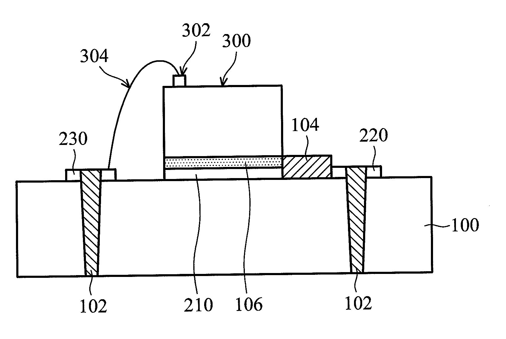
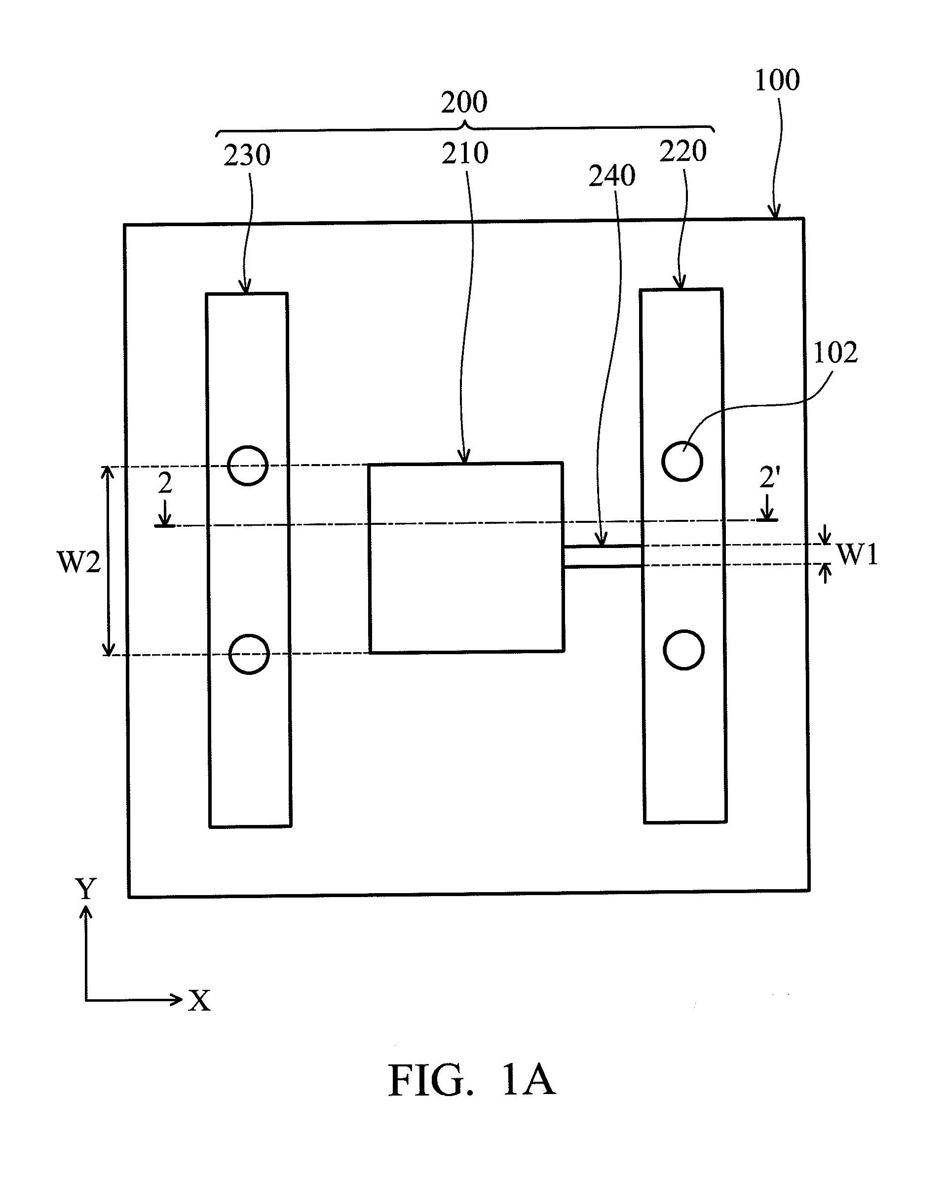
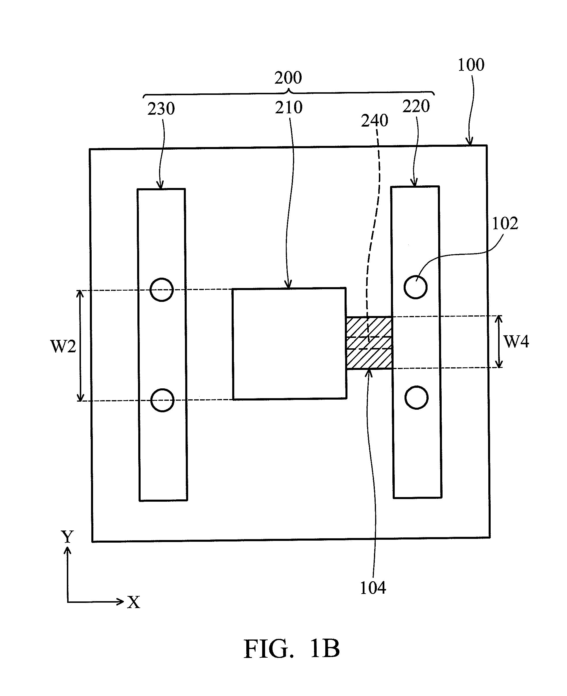
[0017]An exemplary embodiment of the invention provides a conductive pad design for a chip package to prevent solder overflow. FIG. 1A shows a plane view of a conductive pad 200 for a chip package according to an embodiment of the invention. The conductive pad 200 is disposed on a substrate 100, having a first portion 210 disposed under a solder layer (not shown), a second portion 220 disposed away from the first portion 210, a third portion 230 disposed away from the first portion 210 and opposite to the second portion 220, and a connective portion 240 disposed between the first portion 210 and the second portion 220. The connective portion 240 has a width W1 narrower...


PUM


Abstract

A chip package and a fabrication method thereof are provided. The chip package includes a substrate and a chip disposed over the substrate. A solder layer is disposed between the chip and the substrate. A conductive pad is disposed between the solder layer and the substrate, wherein the conductive pad includes a first portion disposed under the solder layer, a second portion disposed away from the first portion and a connective portion disposed between the first portion and the second portion. The connective portion has a width which is narrower than a width of the first portion along a first direction perpendicular to a second direction extending from the first portion to the connective portion.

Description

BACKGROUND OF THE INVENTION[0001]1. Field of the Invention[0002]The invention relates to a chip package and more particularly to a conductive pad design of a chip package which prevents solder overflow.[0003]2. Description of the Related Art[0004]In conventional chip packages, a chip, for example a light emitting chip, is soldered on a metal pad through a solder layer by a solder reflow process. The metal pad has a portion covered with the solder layer for soldering with the chip and a portion not covered with the solder layer and the chip. The solder layer is disposed on the portion of the metal pad covered with the chip before the solder reflow process. However, after the solder reflow process, the solder layer overflows from the portion of the metal pad covered with the chip onto the portion not covered with the chip. In such a case, the solder layer between the chip and the metal pad may be insufficient for soldering the chip on the metal pad. Thus, reliability of the convention...

Claims


Application Information

Patent Timeline
IPC IPC(8): H01L23/492H01L21/50
CPCH01L23/49827H01L2924/15787H01L24/32H01L24/33H01L24/48H01L24/73H01L24/83H01L33/62H01L2224/04042H01L2224/32238H01L2224/32506H01L2224/335H01L2224/48227H01L2224/48235H01L2224/73265H01L2224/83192H01L2224/83805H01L2224/83815H01L2924/01029H01L2924/01047H01L2924/0105H01L2924/01079H01L2924/12035H01L2924/14H01L2924/01033H01L2924/01322H01L2924/014H01L2924/0132H01L24/29H01L2224/32225H01L2224/291H01L2224/26175H01L2924/12041H01L2224/48091H01L2224/27013H01L2224/29111H01L2924/1579H01L23/49838H01L2924/00H01L2924/00014H01L2924/00012H01L2924/15747H01L2224/45099H01L2224/45015H01L2924/207
Inventor CHANG, KUO-CHINGKUO, WU-CHENGLIN, TZU-HAN
Owner SEMILEDS OPTOELECTRONICS CO LTD
Why Eureka
Try Eureka