Switching power source apparatus
a power source and switch technology, applied in the direction of electric variable regulation, process and machine control, instruments, etc., can solve the problems of deteriorating the load regulation characteristic, affecting the operation of the switch, and prolonging the on timing of the high-side mosfet b>11/b> delays, etc., to achieve stable operation and good load regulation characteristic
- Summary
- Abstract
- Description
- Claims
- Application Information
AI Technical Summary
Benefits of technology
Problems solved by technology
Method used
Image

Examples
embodiment 1
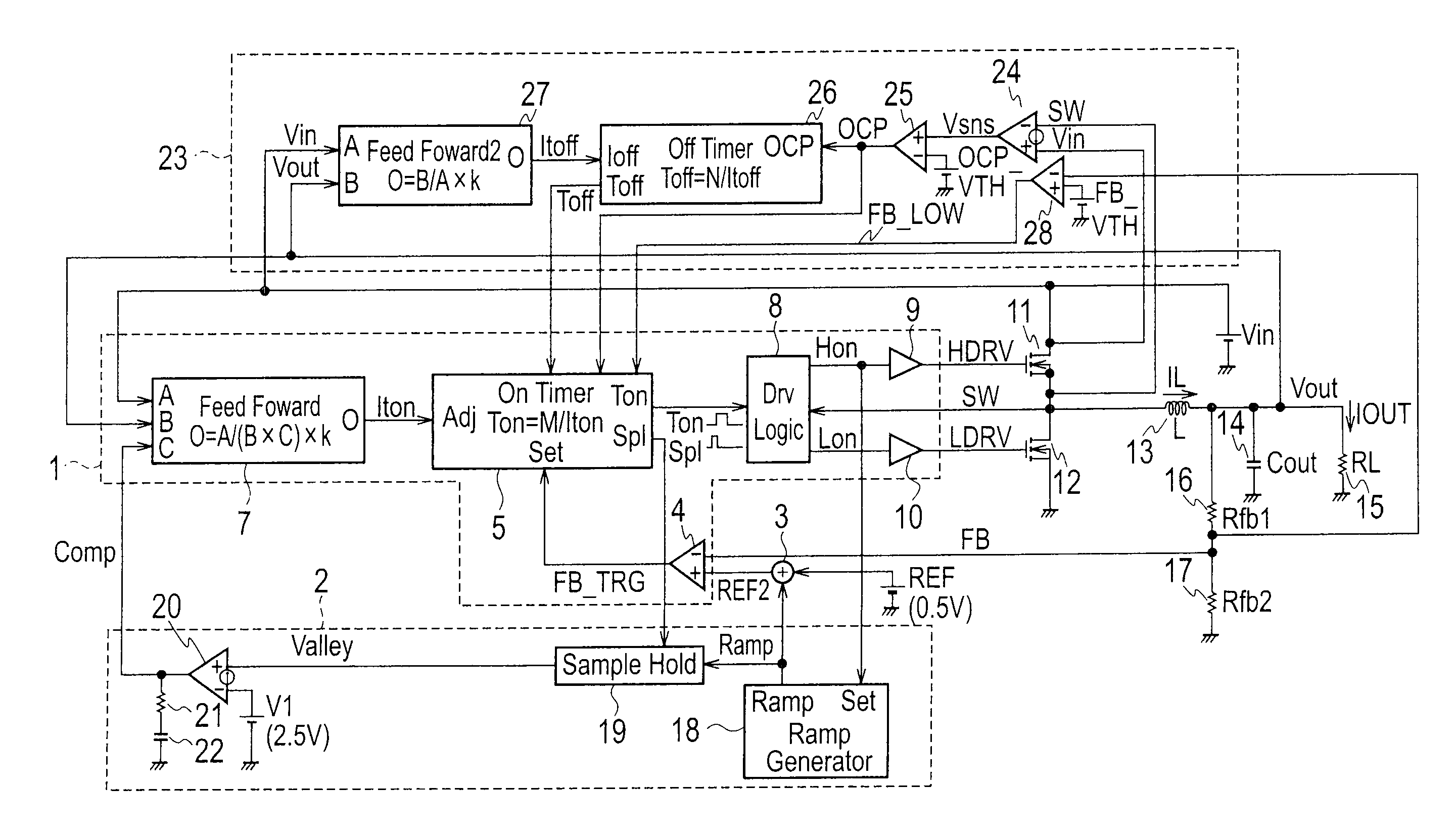
[0044]A switching power source apparatus according to Embodiment 1 of the present invention will be explained with reference to FIG. 3. Parts of FIG. 3 that are similar to those of the related art of FIG. 1 are represented with like reference numerals to avoid a repetition of explanation.
[0045]In FIG. 3, the switching power source apparatus according to the present embodiment includes a first feedback controller 1, a second feedback controller 2, a superposing circuit 3, a high-side MOSFET 11, a low-side MOSFET 12, an inductor 13, an output smoothing capacitor 14, an output load 15, feedback res stars 16 and 17, and an overcurrent protection circuit 23.
[0046]The first feedback controller 1 includes a feedback comparator 4, a feedforward circuit 7, an ON timer 5, a drive logic 8, a high-side driver 9, and a low-side driver 10.
[0047]The second feedback controller 2 includes a ramp generator 18, a sample hold circuit 19, an error amplifier 20, a phase compensation resistor 21, and a ph...
embodiment 2
[0121]FIG. 17 is a circuit diagram illustrating a switching power source apparatus according to Embodiment 2 of the present invention. Embodiment 2 differs from Embodiment 1 illustrated in FIG. 3 in that Embodiment 2 employs an overcurrent protection circuit 23b instead of the overcurrent protection circuit 23. The remaining part of Embodiment 2 is the same as that of Embodiment 1. In the overcurrent protection circuit 23b of the present embodiment, input terminals of a current sense amplifier 24 are connected to the drain and source of the low-side MOSFET 12 instead of those of the high-side MOSFET 11 and there is additionally arranged a second sample hold circuit 29. The low-side MOSFET 12 corresponds to the low-side switch as stipulated in the claims and is connected between the inductor 13 and the ground.
[0122]The current sense amplifier 24 generates, based on a drain-source potential difference of the low-side MOSFET 12 just after the low-side MOSFET 12 turns on, a signal Vsns2...
PUM
 Abstract
Description
Claims
Application Information
 - R&D Engineer
- R&D Manager
- IP Professional
- Industry Leading Data Capabilities
- Powerful AI technology
- Patent DNA Extraction
Browse by: Latest US Patents, China's latest patents, Technical Efficacy Thesaurus, Application Domain, Technology Topic.
© 2024 PatSnap. All rights reserved.Legal|Privacy policy|Modern Slavery Act Transparency Statement|Sitemap