Semiconductor device and control method thereof

a technology of semiconductor devices and dielectric devices, applied in the field of semiconductor devices, can solve the problems of increasing reducing and difficulty in arranging sense amplifiers, so as to prevent the influence of the effect of sufficiently suppressing the coupling noise between adjacent bit lines and improving the sensing margin of the sense amplifier

Inactive Publication Date: 2012-03-15
LONGITUDE SEMICON S A R L
View PDF3 Cites 17 Cited by
  • Summary
  • Abstract
  • Description
  • Claims
  • Application Information

AI Technical Summary

Benefits of technology

[0010]As described above, according to the invention, when the coupling capacitance between adjacent bit lines increases due to the miniaturization of the manufacturing scale, the coupling noise between the adjacent bit lines can be sufficiently suppressed by, for example, amplifying respective signals of two memory cells at different timings in temporally divided two operations (during first and second read periods) using corresponding sense amplifiers in the read operation. Therefore, an effect of improving sensing margin of the sense amplifier can be obtained. Meanwhile, when externally input data is written into the memory cells, writing operation is performed after the amplifying operations thereof during the first and second read periods, and thus an effect of preventing influence of the coupling noise between the adjacent bit lines can be obtained.
[0011]Further, when the sense amplifiers arranged in a zigzag manner are connected to input / output lines, respective sense amplifiers on both sides of the memory cell array can be independently connected to different input / output lines, and thus it is possible to suppress mutual influences of amplifying operations in which respective data of the sense amplifiers are read out at different timings. Furthermore, two word lines corresponding to row addresses of which a predetermined bit is different from each other are simultaneously selected, activation timings of the sense amplifiers are controlled in response to the predetermined bit, and thus an effect of maintaining compatibility with general DRAMs can be obtained.
[0012]As described above, the configuration of the invention is effective for the semiconductor device having the hierarchical bit line structure with the miniaturization of manufacturing scale, particularly in which, an open bit line structure or a single-ended configuration is applied to the memory cell array. In this case, the coupling noise between adjacent global bit lines can be small while reducing the bit line capacitance of each global bit line. Therefore, even if the memory cell capacitance is reduced due to the miniaturization, it is possible to achieve a large capacity semiconductor device capable of obtaining sufficient sensing margin. Further, the invention can be applied to a configuration in which each global sense amplifier is shared by memory cell arrays adjacent to each other, and thereby it is possible to improve the sensing margin without an increase in chip area.

Problems solved by technology

Further, it is difficult to arrange sense amplifiers so that they adapt to the reduced bit line pitch, and therefore an arrangement in which a plurality of sense amplifiers are alternately arranged at both ends of the global bit lines is effective (so-called zigzag alignment).
Accordingly, there arises a problem that when a signal voltage read out from a memory cell by selecting a word line is sensed and amplified by a sense amplifier, the coupling noise between the adjacent bit lines increases so that sensing margin of the sense amplifier decreases.

Method used


Image

  • Semiconductor device and control method thereof
  • Semiconductor device and control method thereof
  • Semiconductor device and control method thereof

Examples


first embodiment

[Modification of First Embodiment]

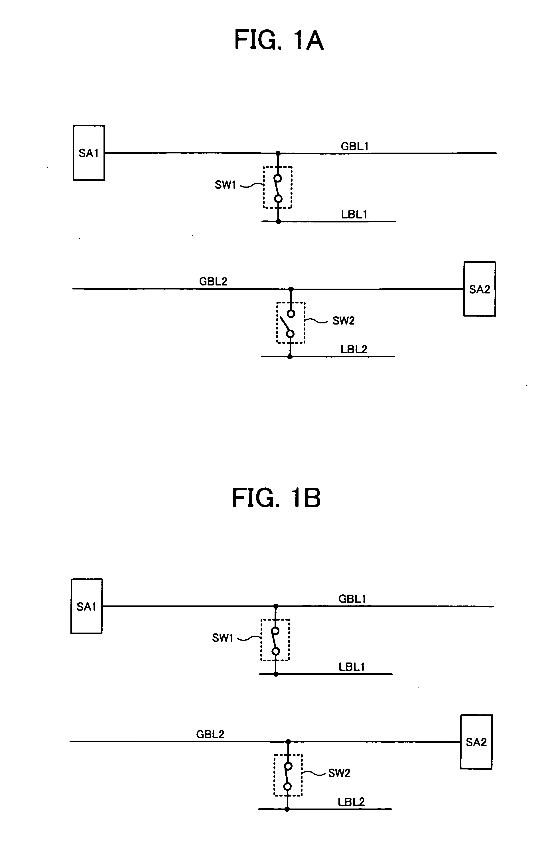
[0052]A modification of the first embodiment will be described, in which the connection control signals LSWE and LSWO can be controlled in the following manner. That is, in an initial period (before the precharge cancellation period T1), the connection control signals LSWE and LSWO are both set into a conductive state (high level). During the selection period T2, the connection control signal LSWO is set into a non-conductive state (low level) and the connection control signal LSWE is maintained in the conductive state (high level). During the selection period T5, the connection control signal LSWE is set into the non-conductive state (low level) and the connection control signal LSWO is set into the conductive state (high level) from the non-conductive state (low level).

second embodiment

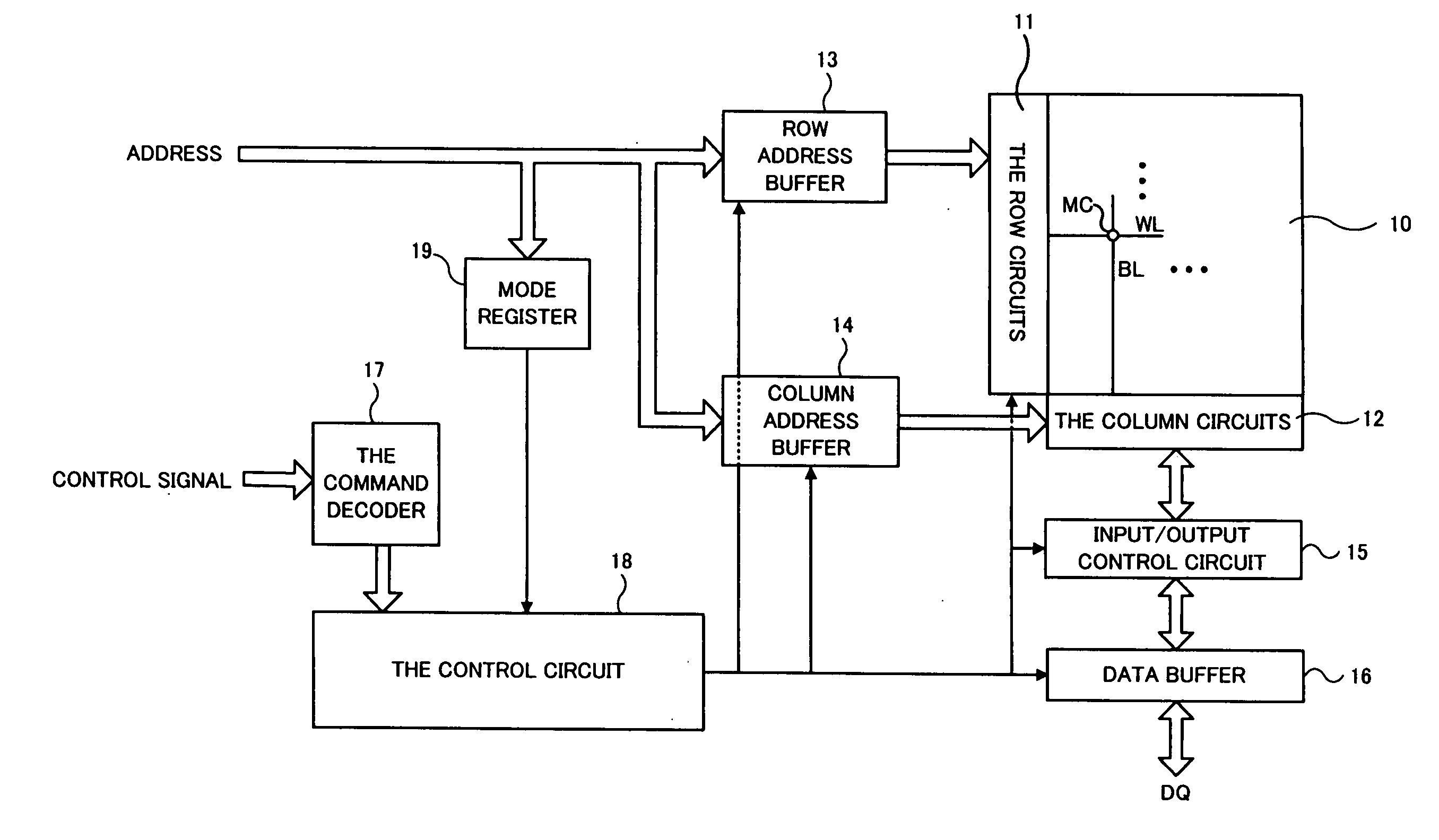
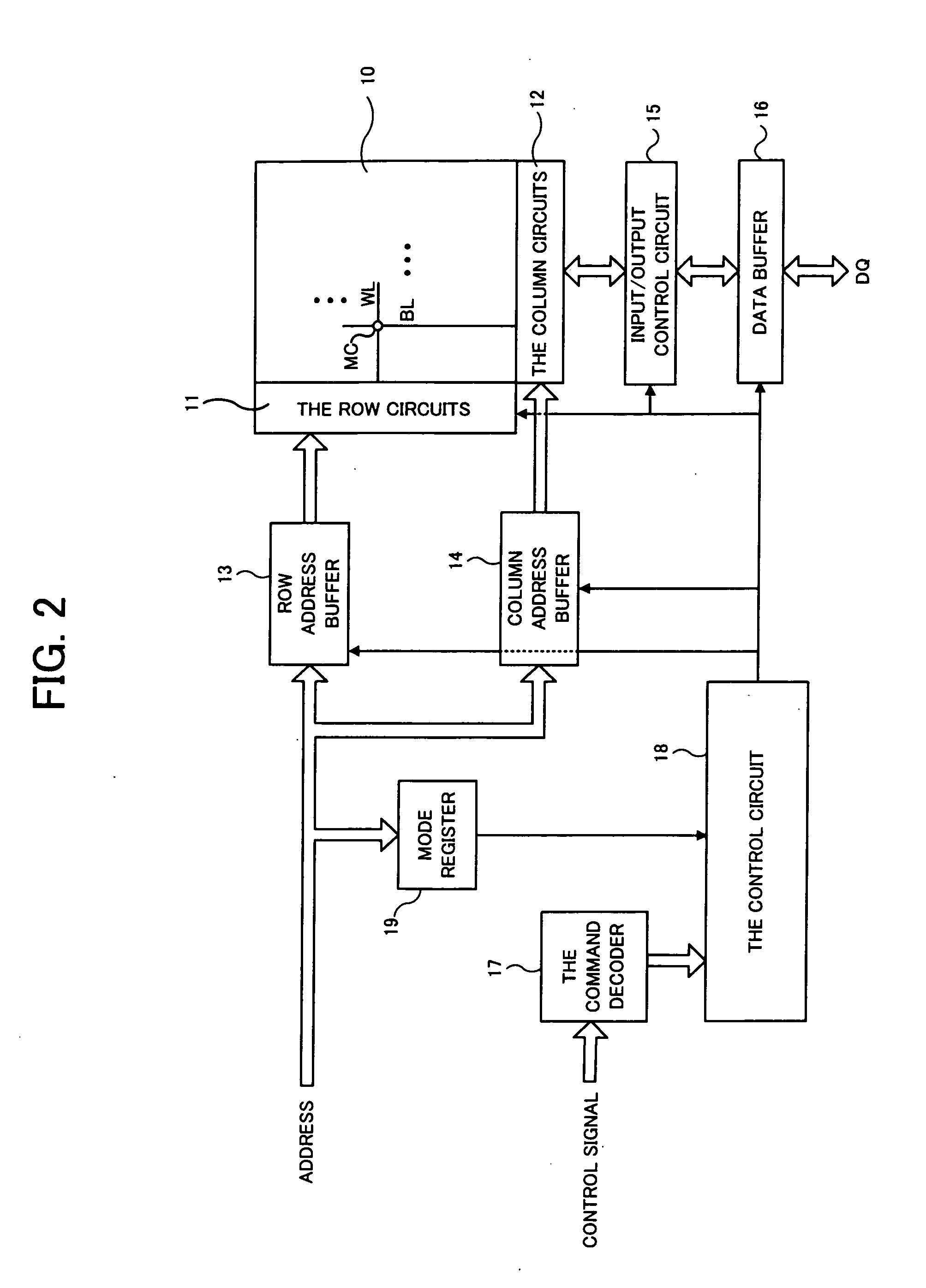
[0053]Next, the DRAM of a second embodiment to which the invention is applied will be described. The entire configuration of the DRAM of FIG. 2 is common in the second embodiment, so description thereof will be omitted. FIG. 7 shows a configuration of the memory cell array 10 and its peripheral portion in the DRAM of the second embodiment, which shows an area corresponding to FIG. 3. As shown in FIG. 7, the memory cell array 10 of the second embodiment employs the hierarchical bit line structure, which is not the open bit line structure as in the first embodiment, and employs a single-ended array configuration using single-ended amplifies. For example, a single-ended local sense amplifier LSA has a configuration in which a gate terminal (input node of the amplifier) of the first transistor constituting the amplifier is connected to the local bit line LBL to which the memory cell MC is connected, and a drain terminal (output node of the amplifier) is connected to the global bit line ...

third embodiment

[0070]Next, the DRAM of a third embodiment to which the invention is applied will be described. FIG. 9 shows a configuration in the DRAM of the third embodiment, which corresponds to the area of FIG. 7 of the second embodiment. The third embodiment has a configuration based on the configuration of FIG. 7 of the second embodiment, in which each global sense amplifier GSA is shared by two global bit lines GBL belonging to adjacent memory cell arrays 10 on both sides. Therefore, PMOS type transistors Q30a, Q30b, Q40a and Q40b and NMOS type transistors Q33a, Q33b, Q4a and Q43b are arranged instead of the transistors Q30 and Q40 of FIG. 7. In addition, portions of the local sense amplifier LSA and the transistors Q31, Q32, Q41 and Q42 are the same as in FIG. 7.

[0071]In FIG. 9, one global sense amplifier GSA(E) is selectively connected to the global bit lines GBL(E) on both sides by the transistor Q33a having a gate applied with a connection control signal GSWRE and the transistor Q33b ha...


PUM


Abstract

A semiconductor device has a hierarchical bit line structure and comprises first and second local bit lines transmitting first and second signals of first and second memory cells corresponding to a selected word line, and first and second global bit lines electrically connected to the first and second local bit lines through first and second switches, first and second sense amplifiers connected to the first and second global bit lines, and a control circuit. During a first period after the first and second memory cells are simultaneously accessed, the control circuit controls the first switch to conduction state so that the first sense amplifier amplifies the first signal and controls the second switch to non conduction state. During a second period after sensing of the first sense amplifier finishes, the control circuit controls the second switch to conduction state so that the second sense amplifier amplifies the second signal.

Description

BACKGROUND OF THE INVENTION[0001]1. Field of the Invention[0002]The present invention relates to a semiconductor device comprising a memory cell array having a bit line structure hierarchized using global bit lines and local bit lines, and a control method thereof.[0003]2. Description of Related Art[0004]In recent years, miniaturization of a memory cell array has been achieved in semiconductor devices such as DRAM, and thus in order to overcome a performance problem caused by an increase in the number of memory cells connected to a bit line, a configuration in which the bit lines are hierarchized into global bit lines and local bit lines has been proposed (for example, refer to Japanese Patent Application Laid-open No. 2008-262632 (U.S. Pat. No. 7,697,358 B2)). It is required to reduce memory cell size to, for example, 6F2 or 4F2 (“F” is minimum manufacturing scale), and the bit line pitch in this case needs to be'set to 2F that is a manufacturing limit. In general, when employing t...

Claims


Application Information

Patent Timeline
Patent Type & Authority Applications(United States)
IPC IPC(8): G11C7/10
CPCG11C2207/005G11C11/4097
Inventor KAJIGAYA, KAZUHIKO
Owner LONGITUDE SEMICON S A R L
Why Eureka
Try Eureka