Method for forming a pattern and a semiconductor device manufacturing method
a manufacturing method and pattern technology, applied in the field of pattern formation and semiconductor device manufacturing methods, can solve the problems of plasma damage, other problems, and difficulty in controlling the shape of the pattern
- Summary
- Abstract
- Description
- Claims
- Application Information
AI Technical Summary
Benefits of technology
Problems solved by technology
Method used
Image

Examples
Embodiment Construction
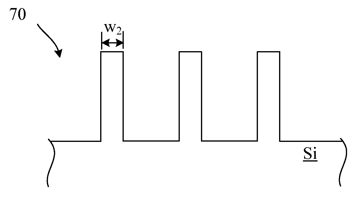
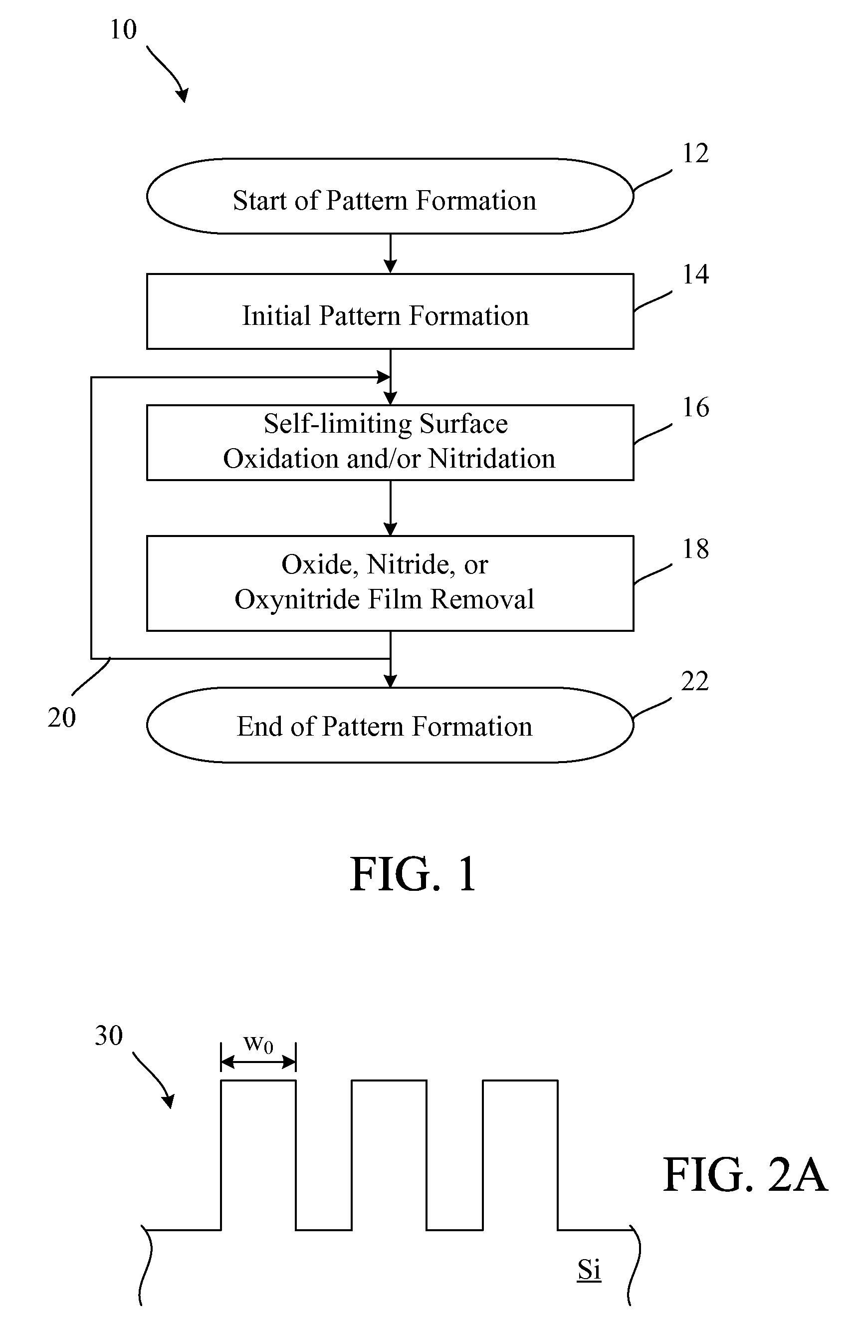
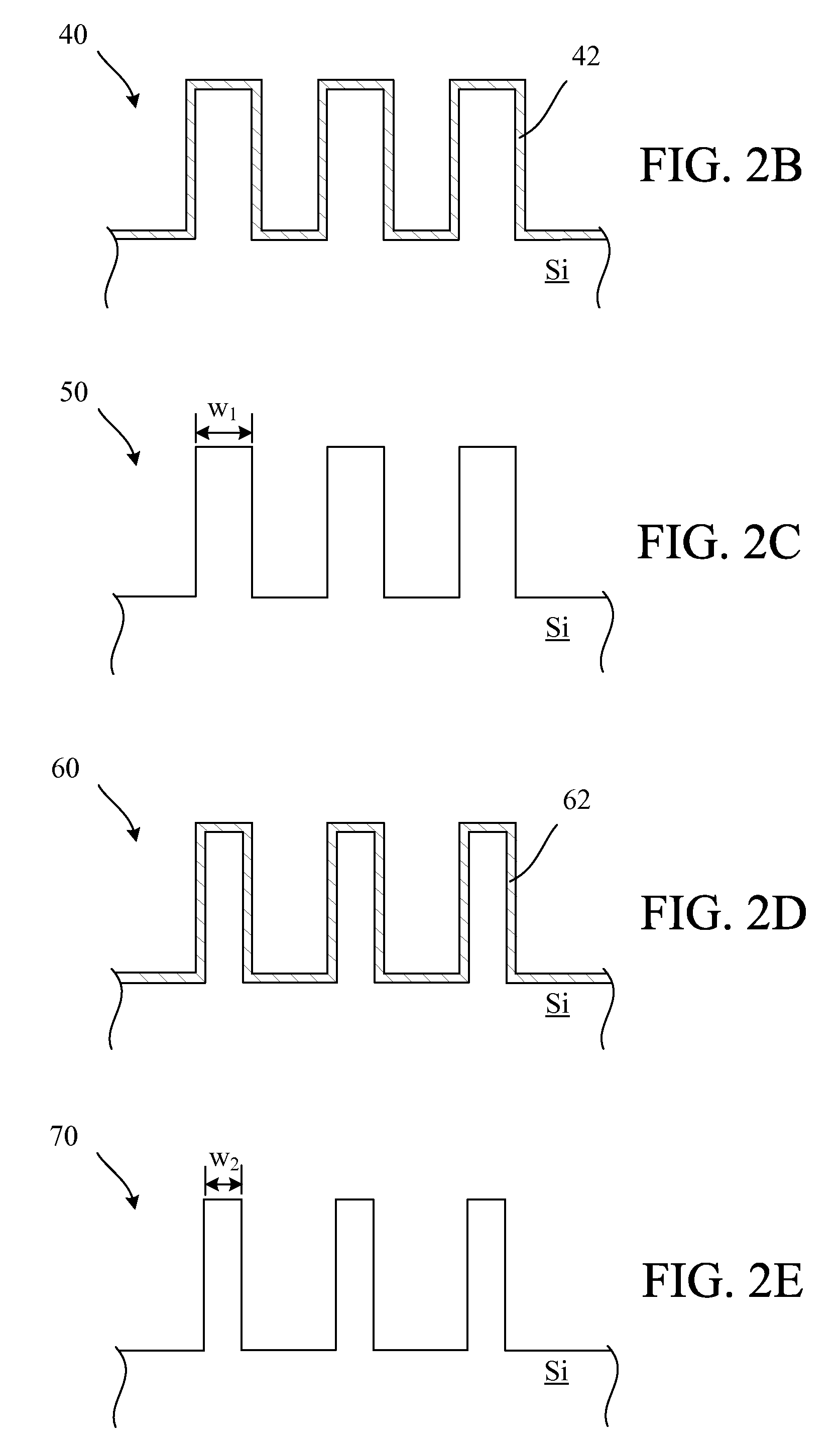
[0016]Embodiments of the invention describe methods to thin or shrink features made of Si, Si-containing materials (e.g., SiN), metals (e.g., Al), or metal nitrides. The method combines self-limited, highly conformal, oxidation, nitridation, or oxidation and nitridation with subsequent oxide, nitride, or oxynitride film removal (e.g., COR), performed in alternating sequences, to thin or shrink a feature. The methods provide an etch process with digital control over material removal that includes excellent controllability with minimal rounding or distortion.
[0017]In one embodiment, a feature is patterned using traditional lithography and a standard etch process is designed to create a feature larger than the desired feature that has the desired shape. The feature is then further processed using a self-limited oxidation and / or nitridation process that can include exposure to vapor phase ozone (VPO), exposure to atomic oxygen generated by non-ionizing electromagnetic (EM) radiation (...
PUM
 Abstract
Description
Claims
Application Information
 - R&D Engineer
- R&D Manager
- IP Professional
- Industry Leading Data Capabilities
- Powerful AI technology
- Patent DNA Extraction
Browse by: Latest US Patents, China's latest patents, Technical Efficacy Thesaurus, Application Domain, Technology Topic.
© 2024 PatSnap. All rights reserved.Legal|Privacy policy|Modern Slavery Act Transparency Statement|Sitemap