Apparatus and methods for forming film pattern

a technology of film pattern and pattern, applied in the direction of forming conductive pattern, inking apparatus, superconductor device, etc., to achieve the effect of reducing line width, simple steps, and efficient film thickness

Inactive Publication Date: 2006-02-07
SEIKO EPSON CORP
View PDF4 Cites 83 Cited by
  • Summary
  • Abstract
  • Description
  • Claims
  • Application Information

AI Technical Summary

Benefits of technology

[0030]It is also an object to provide a fine, thick conductive film wiring, which provides advantages with respect to the electrical conduction and is unlikely to bring about problems such as breaks and short circuits.
[0065]According to the present invention, a fine, thick conductive film wiring, which provides advantages with respect to the electrical conduction and is unlikely to bring about problems, such as breaks and short circuits.

Problems solved by technology

This lithography method requires large-scale equipment, such as a vacuum apparatus, and complicated steps.
Therefore, the efficiency of use of the material is about several percentages, the most of the material have to be discarded, and the manufacturing cost can be expensive.
In other words, when the conductive fine particles are not overlapped, the portions where the conductive fine particles are not made contact with each other bring about breaks, etc.
Furthermore, when increase in thickness is insufficient, electrical resistance is increased and, therefore, the conductivity of the wiring becomes inferior.
However, regarding the method in which the substrate is directly pattern-coated by the ink-jet method with the liquid containing conductive fine particles being dispersed, since the liquid containing conductive fine particles being dispersed is used, there is a limit of the quantity of the conductive fine particles that can be applied by coating through discharge of a fixed quantity of the liquid from the viewpoint of viscosity, etc., during discharge.
On the other hand, when it is intended to discharge the liquid in large quantities at a time, it becomes difficult to control the position of formation of the wiring.
In addition, the line width of the wiring becomes large contrary to requirements for integration of electronic circuits, etc.
However, such a bank has to be formed using photolithography and, therefore, an increase in cost is brought about.
However, regarding this method, since a step of forming patterns of the lyophilic portion and the liquid-repellent portion by using a mask, etc., is required and, in addition, a step of providing alignment marks for precisely applying a coating on the lyophilic pattern is also required, the process becomes complicated.
In addition, since the discharge is performed onto the lyophilic portion and, the droplets spread, it becomes difficult to form a conductive film with an increased film thickness.
However, it becomes difficult to collect the liquid within the lyophilic portion unless the liquid-repellent property of the liquid-repellent portion with respect to the liquid is increased by a large degree.
Furthermore, the line width of the wiring to be formed is limited to the width of the lyophilic portion of the substrate.
As described above, generation of the bulge brings about a fatal defect in performance of the conductive film wiring.
However, although the method according to the Japanese Patent Application No. 2001-193679 prevented generation of the bulge, it did not exhibit an adequate effect of preventing the liquid containing conductive fine particles being dispersed from wetting and spreading after being hit onto the substrate because the liquid-repellent property of the substrate was 60 degrees or less and was not so large.
Furthermore, in the case where another coating was applied after the liquid was dried, since the liquid-repellent property of the substrate was 60 degrees or less and was not so large, difference in the liquid-repellent property from the portion which became lyophilic after the liquid was dried was not adequate.
Consequently, when the quantity of the liquid was excessive in application of another coating, there were problems in that the liquid did not remain at the portion where the liquid had been dried previously, and was likely to flow down to the substrate and, therefore, the line width was increased.
However, regarding formation of the silicon thin film pattern by these CVD methods and the photolithography, further improvements have been expected with respect to the following points in terms of the process.(1) Since a vapor phase reaction is used, particles of silicon are generated in the vapor phase and, therefore, production yield is low due to pollution of the apparatus and generation of foreign matters.(2) Since the raw material is gaseous, a silicon thin film with a uniform thickness is unlikely to be produced on a substrate having convexities and concavities on the surface.(3) Since the formation speed of the film is low, the productivity is low.(4) In the plasma CVD method, complicated and expensive high-frequency generators, vacuum apparatuses, etc., are required.(5) Regarding photolithography, the process is complicated, the efficiency of use of the raw material is low, and large quantities of wastes, such as resists and etchants are generated.
In terms of the material, since gaseous silicon hydride having high toxicity and high reactivity is used, it is difficult to handle and, in addition, a hermetically sealed vacuum apparatus is required because of the material being gaseous.
In general, these apparatuses are large-scale, the apparatuses themselves are expensive and, in addition, high cost of the product is brought about because a great deal of energy is consumed for a vacuum system and a plasma system.
However, regarding this method, since a step of forming patterns of the lyophilic portion and the liquid-repellent portion by using a mask, etc., is required and, in addition, a step of providing alignment marks for precisely applying a coating on the lyophilic pattern is also required, the process becomes complicated.
In addition, although the silicon film pattern is required to also have a somewhat large film thickness in order to keep the uniformity of the film, since the discharge is performed onto the lyophilic portion, the droplets spread by wetting and, therefore, it becomes difficult to increase the film thickness.
However, it becomes difficult to collect the liquid within the lyophilic portion unless the liquid-repellent property of the liquid-repellent portion with respect to the liquid is increased by a large degree.

Method used


Image

  • Apparatus and methods for forming film pattern
  • Apparatus and methods for forming film pattern
  • Apparatus and methods for forming film pattern

Examples


first embodiment

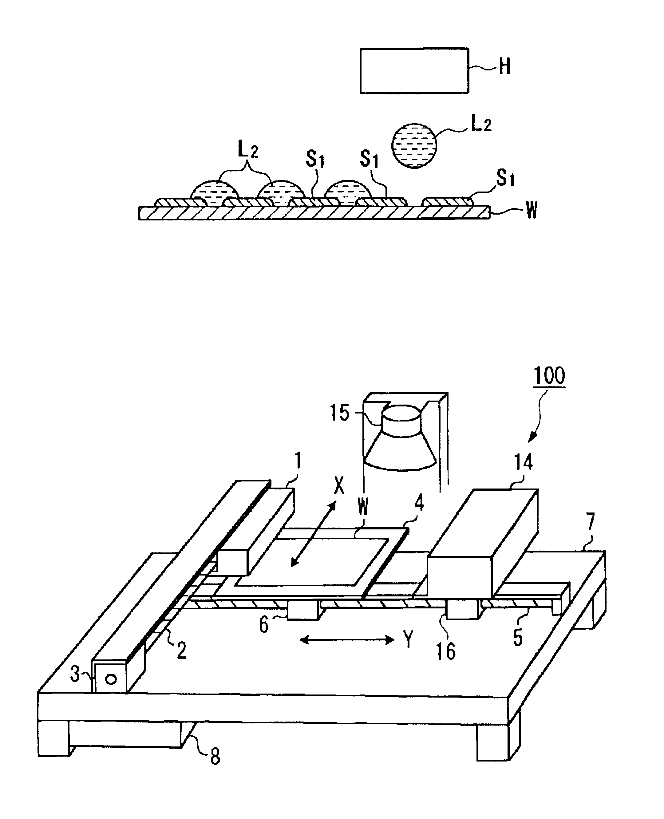
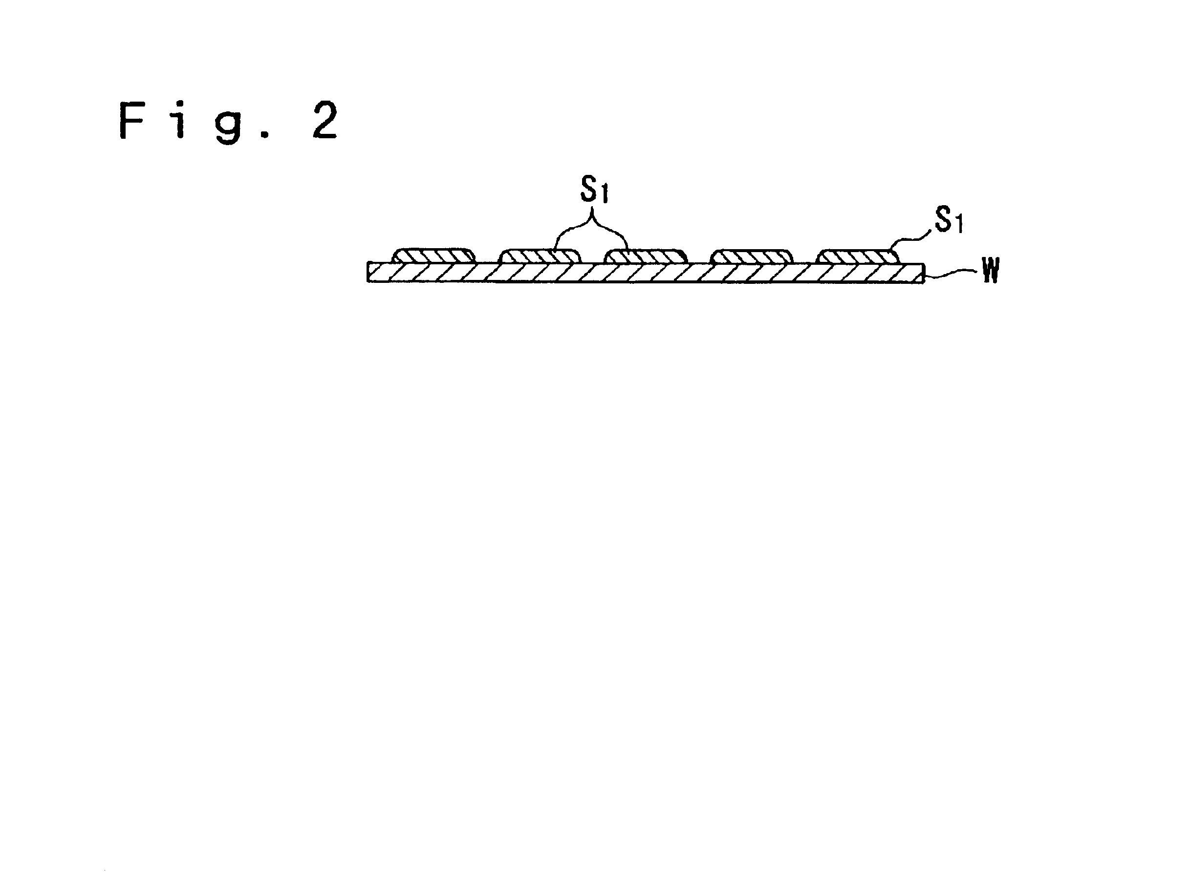
[0085]As the first embodiment, a method for forming a wiring, which is an example of the method for forming a film pattern of the present invention, will be described. The method for forming a wiring according to the present embodiment is composed of a surface treatment step, a discharging step, and a heat treatment / optical treatment step. Among them, the discharging step is composed of a dispersion preparation step, the first discharging step, the second discharging step, and the third discharging step. Each step will be described below.

[0086]Various materials, such as Si wafers, quartz glass, glass, plastic films, and metal plates, can be used as a substrate on which a conductive film wiring is to be formed. Those in which semiconductor films, metal films, dielectric films, organic films, and the like, are formed as substrate layers on the surfaces of these various material substrates may be used as the substrate on which the conductive film wiring is to be formed.

[0087]The surfac...

third embodiment

[0162]As the third embodiment, a method for forming a silicon film pattern, which is an example of the method for forming a film pattern of the present invention, will be described. The method for forming a silicon film pattern according to the present embodiment is composed of a surface treatment step, a discharging step, and a heat treatment / optical treatment step. Among them, the discharging step is composed of a solution preparation step, the first discharging step, the second discharging step, and the third discharging step. Each step will be described below.

[0163]Various materials, for example, Si wafers, quartz glass, glass, plastic films, and metal plates, can be used as a substrate on which a silicon thin film pattern is to be formed. Those in which semiconductor films, metal films, dielectric films, organic films, etc., are formed as substrate layers on the surfaces of these various material substrates may be used as the substrate on which the silicon thin film pattern is ...

fourth embodiment

[0190]As the fourth embodiment, a liquid crystal device, which is an example of the electro-optic apparatus of the present invention, will be described. FIG. 8 is a diagram showing a two-dimensional layout of signal electrodes, etc., on a first substrate of the liquid crystal device according to the present embodiment. The liquid crystal device according to the present embodiment is roughly composed of this first substrate, a second substrate (not shown in the drawing) provided with scanning electrodes, etc., and a liquid crystal (not shown in the drawing) injected between the first substrate and the second substrate.

[0191]As shown in FIG. 8, a plurality of signal electrodes 310 . . . are installed in the shape of a multiplex matrix in a pixel region 303 on the first substrate 300. In particular, each of the signal electrodes 310 . . . is composed of a plurality of pixel electrode portions 310a . . . installed corresponding to individual pixels and signal wirings 310b . . . connecti...


PUM


Abstract

The invention provides a method for forming a film pattern, in which a method for forming a film pattern by the ink-jet method is improved, an increase in film thickness is achieved efficiently with simple steps, a requirement for a decrease in line width is met and, in addition, problems such as breaks and short circuits are not brought about when a conductive film is made. The method can include a first discharging step, wherein droplets are discharged in the whole film formation region with a pitch larger than the diameter of the droplet after being hit onto the substrate. In the second discharging step, droplets are discharged at positions in the whole film formation region different from the discharge positions in the first discharging step with the same pitch as that in the first discharging step. In the third discharging step, droplets are discharged in the whole film formation region with a pitch smaller than the pitch in the first discharging step. The substrate is treated beforehand in order to have the contact angle of 60 degrees or more with respect to the droplets.

Description

BACKGROUND OF THE INVENTION[0001]1. Field of Invention[0002]The present invention relates to a method for forming film patterns, such as a conductive film wiring and a silicon film pattern, used for such as wirings of electrodes, antennas, electronic circuits, and integrated circuits, and an apparatus for forming the same. The present invention also relates to a conductive film wiring, an electro-optical apparatus, electronic equipment, and a non-contact card medium.[0003]2. Description of Related Art[0004]Currently, lithography methods, for example, are used in the manufacture of wirings used for electronic circuits, integrated circuits, or the like. In such lithography methods, a coating of a photosensitive material referred to as resist is applied on a substrate coated beforehand with a conductive film, a circuit pattern is irradiated and is developed, the conductive film is etched in accordance with the resist pattern and, therefore, a wiring is formed. This lithography method r...

Claims


Application Information

Patent Timeline
Patent Type & Authority Patents(United States)
IPC IPC(8): B41J29/393B41J2/01B41J3/407H01L21/288H01L21/768H05K3/10H05K3/12
CPCB41J3/407H05K3/125H01L21/288B41J2202/09H05K2203/1476
Inventor HASHIMOTO, TAKASHIFURUSAWA, MASAHIRO
Owner SEIKO EPSON CORP
Why Eureka
Try Eureka