Multi-level memory arrays with memory cells that employ bipolar storage elements and methods of forming the same

a memory array and memory cell technology, applied in the field of memory arrays, can solve the problems of difficult fabrication of memory devices from rewriteable resistivity-switching materials

Active Publication Date: 2012-04-19
SANDISK TECH LLC
View PDF4 Cites 47 Cited by
  • Summary
  • Abstract
  • Description
  • Claims
  • Application Information

AI Technical Summary

Benefits of technology

[0017]In an eleventh aspect of the invention, a method of forming a memory cell is provided that includes (1) forming a storage element by (a) forming a first conductive layer above a substrate; (b) forming an RRS layer above the first conductive layer; and (c) forming a second conductive layer above the RRS layer, at least one o

Problems solved by technology

However, fabricating memory devices from rewriteable resistivity-switching materials is difficult; and

Method used


Image

  • Multi-level memory arrays with memory cells that employ bipolar storage elements and methods of forming the same
  • Multi-level memory arrays with memory cells that employ bipolar storage elements and methods of forming the same
  • Multi-level memory arrays with memory cells that employ bipolar storage elements and methods of forming the same

Examples


Embodiment Construction

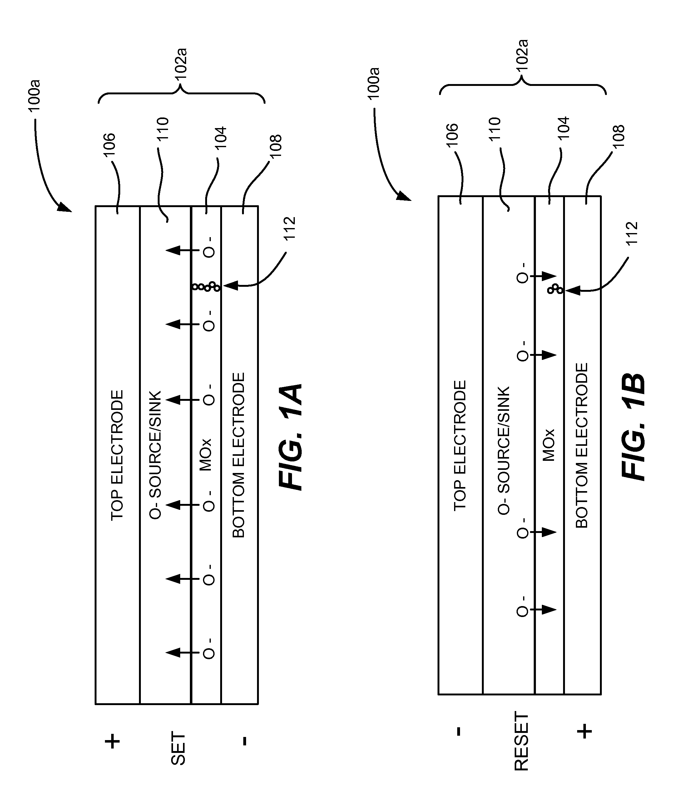
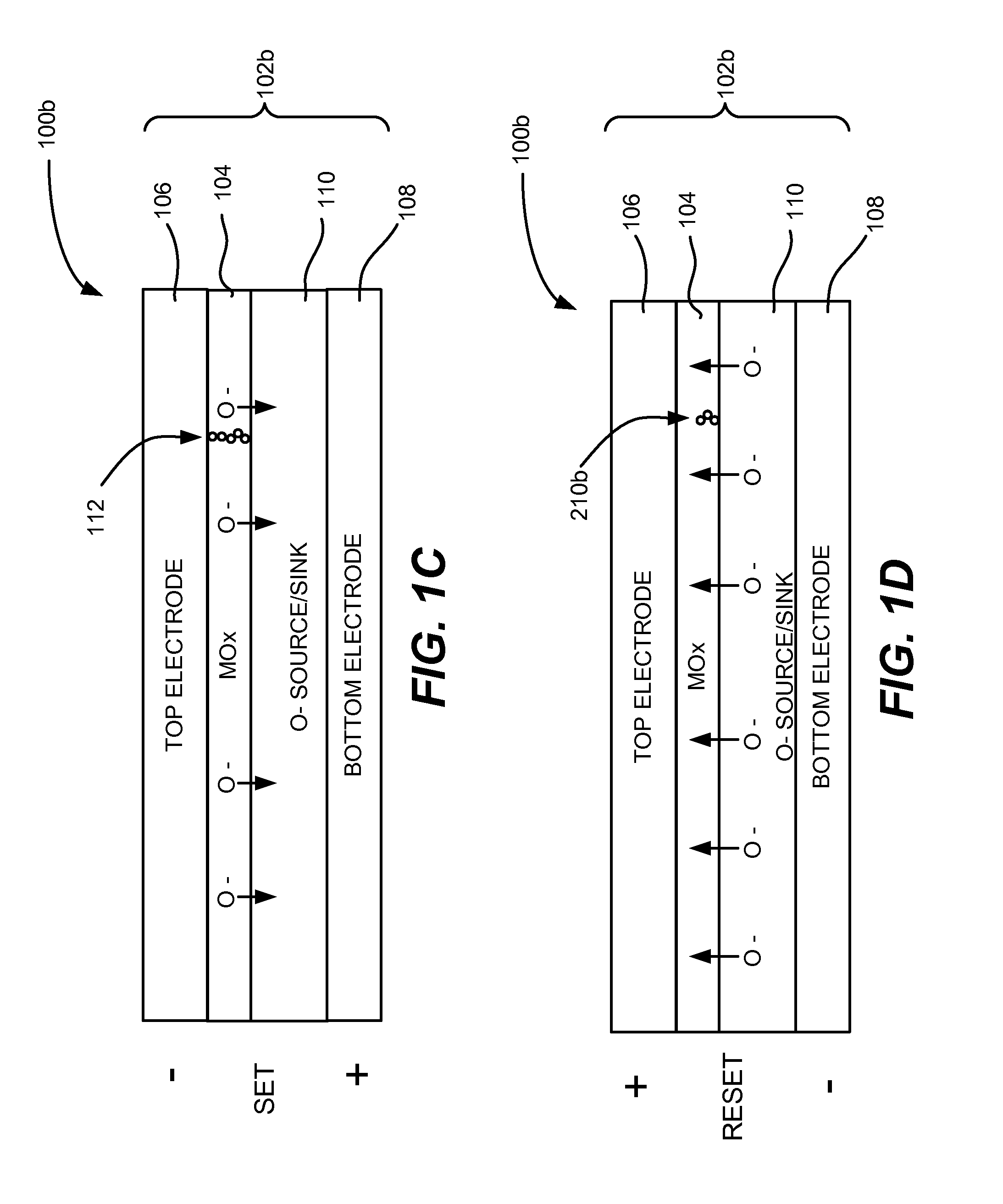
[0034]A metal-insulator-metal (MIM) stack formed from a reversible resistivity switching (RRS) material sandwiched between two metal or otherwise conducting layers may serve as a resistance-switching element for a memory cell. The two conducting layers may serve as the top and bottom electrodes of the resistance-switching element, and may be used to apply an electric field across the RRS material that changes the resistivity of the RRS material from a high value to a low value and vice versa.

[0035]Unipolar MIM stacks employ similar materials on each side of the RRS material, such as the same or similar electrode materials, and generally operate the same independent of which electrode is biased positively or negatively. For some RRS materials, such as metal oxides, unipolar MIM stacks may not switch reliably and may suffer from low yield (e.g., due to set and reset operations being performed using the same voltage polarity with little separation between the set and reset voltages). A...


PUM


Abstract

In some embodiments, a memory array is provided that includes (1) a first memory cell having (a) a first conductive line; (b) a first bipolar storage element formed above the first conductive line; and (c) a second conductive line formed above the first bipolar storage element; and (2) a second memory cell formed above the first memory cell and having (a) a second bipolar storage element formed above the second conductive line; and (b) a third conductive line formed above the second bipolar storage element. The first and second memory cells share the second conductive line; the first bipolar storage element has a first storage element polarity orientation within the first memory cell; the second bipolar storage element has a second storage element polarity orientation within the second memory cell; and the second storage element polarity orientation is opposite the first storage element polarity orientation. Numerous other aspects are provided.

Description

RELATED APPLICATIONS[0001]The present application is related to the following U.S. Patent Applications, each of which is hereby incorporated by reference herein in its entirety:[0002]U.S. patent application Ser. No. ______, filed herewith, and titled “BIPOLAR STORAGE ELEMENTS FOR USE IN MEMORY CELLS AND METHODS OF FORMING THE SAME” (Docket No. MXA-414); and[0003]U.S. patent application Ser. No. ______, filed herewith, and titled “MEMORY CELLS HAVING STORAGE ELEMENTS THAT SHARE MATERIAL LAYERS WITH STEERING ELEMENTS AND METHODS OF FORMING THE SAME” (Docket No. MXA-420).FIELD OF THE INVENTION[0004]The present invention relates to memory arrays, and more particularly to multi-level memory arrays with memory cells that employ bipolar storage elements and methods of forming the same.BACKGROUND OF THE INVENTION[0005]Non-volatile memories formed from reversible resistivity-switching materials are known. For example, U.S. patent application Ser. No. 11 / 125,939, filed May 9, 2005 and titled ...

Claims


Application Information

Patent Timeline
IPC IPC(8): H01L45/00H01L21/02
CPCG11C11/5685H01L45/1608G11C13/0069G11C2013/0073G11C2213/55G11C2213/56G11C2213/71G11C2213/72H01L45/08H01L45/1233H01L45/146H01L45/16H01L27/2409H01L27/2463H01L27/2481H01L45/1253G11C13/0007H10B63/20H10B63/80H10B63/84H10N70/24H10N70/801H10N70/011H10N70/826H10N70/8833H10N70/20H10N70/021H10N70/841
Inventor CHEN, YUNG-TINMIHNEA, ANDREISCHEUERLEIN, ROY E.FASOLI, LUCA
Owner SANDISK TECH LLC
Why Eureka
Try Eureka