
Scalable multi-functional and multi-level nano-crystal non-volatile memory device

a memory device, nano-crystal technology, applied in semiconductor devices, instruments, electrical devices, etc., can solve the problems of volatile dram cells, data loss, and custom technologies that are typically not compatible with each other, and achieve the effect of increasing the non-volatileness of the cell

Active Publication Date: 2007-03-08
MICRON TECH INC
View PDF5 Cites 49 Cited by
  • Summary
  • Abstract
  • Description
  • Claims
  • Application Information

AI Technical Summary

Benefits of technology

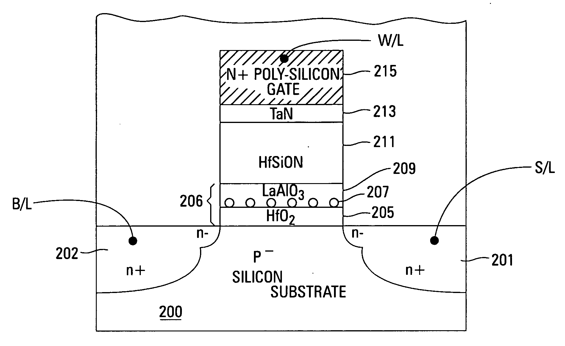
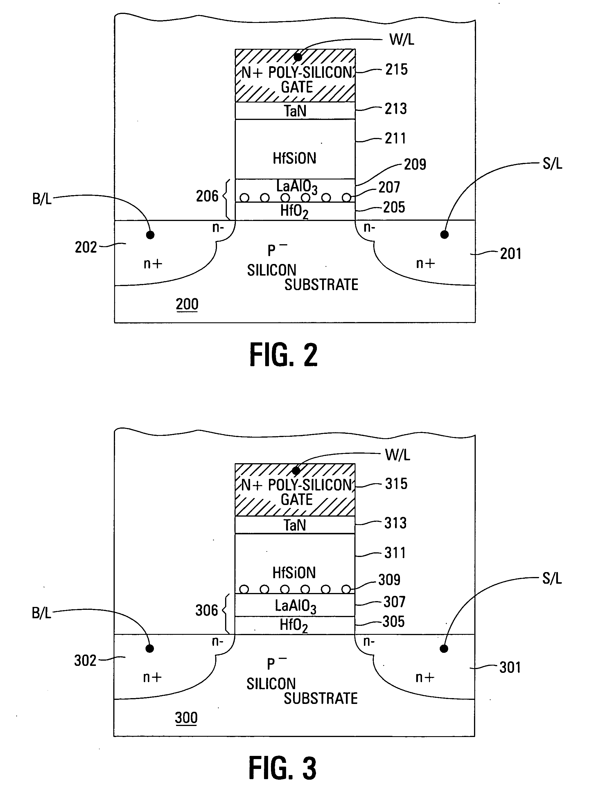
[0015] A charge blocking layer is formed over the tunnel insulator. A control gate is formed over the charge blocking layer. A discrete trapping layer is embedded in either the tunnel insulator or the charge blocking layer. The location of the trapping layer determines the level of non-volatility of the memory cell. The further the trap layer is formed from the silicon / insulator interface, the greater the non-volatility of the cell. The discrete trapping layer is comprised of nano-crystals that are uniform in distribution and size. In one embodiment, the nano-crystals are germanium.

Problems solved by technology

DRAM cells are volatile and therefore lose data when the power is removed.
These memories require custom technologies that are typically not compatible to each other due to different cell design, fabrication techniques, and material characteristics.
Both DRAM and floating gate flash consume relatively high power compared to other memory technologies.
Another problem with these technologies is scalability.
The DRAM has capacitor scalability problems while the flash has voltage and coupling noise scalability problems.
Additionally, with progressive scaling of feature size, fundamental device leakage issues such as short-channel effects and gate dielectric leakage will need to be contained in order to take advantage of scaling.
However, these types of devices can exhibit limited retention and small values for the memory window, thus limiting their application potential and scalability for non-volatile memory.
The threshold window of memory devices using nano-crystals is also adversely affected by the separation of the nano-crystals if the relative distances between the nano-crystals are random.

Method used


Image

  • Scalable multi-functional and multi-level nano-crystal non-volatile memory device
  • Scalable multi-functional and multi-level nano-crystal non-volatile memory device
  • Scalable multi-functional and multi-level nano-crystal non-volatile memory device

Examples


Embodiment Construction

[0028] In the following detailed description of the invention, reference is made to the accompanying drawings that form a part hereof and in which is shown, by way of illustration, specific embodiments in which the invention may be practiced. In the drawings, like numerals describe substantially similar components throughout the several views. These embodiments are described in sufficient detail to enable those skilled in the art to practice the invention. Other embodiments may be utilized and structural, logical, and electrical changes may be made without departing from the scope of the present invention. The following detailed description is, therefore, not to be taken in a limiting sense, and the scope of the present invention is defined only by the appended claims and equivalents thereof. The terms wafer or substrate used in the following description include any base semiconductor structure. Both are to be understood as including silicon-on-sapphire (SOS) technology, silicon-on-...


PUM


Abstract

A multi-functional and multi-level memory cell is comprised of a tunnel layer formed over a substrate. In one embodiment, the tunnel layer is comprised of two layers such as HfO2 and LaAlO3. A charge blocking layer is formed over the tunnel layer. In one embodiment, this layer is formed from HfSiON. A control gate is formed over the charge blocking layer. A discrete trapping layer is embedded in either the tunnel layer or the charge blocking layer, depending on the desired level of non-volatility. The closer the discrete trapping layer is formed to the substrate / insulator interface, the lower the non-volatility of the device. The discrete trapping layer is formed from nano-crystals having a uniform size and distribution.

Description

TECHNICAL FIELD OF THE INVENTION [0001] The present invention relates generally to memory devices and in particular the present invention relates to DRAM and non-volatile memory devices. BACKGROUND OF THE INVENTION [0002] Memory devices are typically provided as internal, semiconductor, integrated circuits in computers or other electronic devices. There are many different types of memory including random-access memory (RAM), read only memory (ROM), non-volatile, floating gate NOR / NAND flash memory, and dynamic random access memory (DRAM). [0003] Flash memories may use floating gate technology or trapping technology in order to store data in the form of charges. Floating gate cells include source and drain regions that are laterally spaced apart to form an intermediate channel region. The source and drain regions are formed in a common horizontal plane of a silicon substrate. The floating gate, typically made of doped polysilicon, is disposed over the channel region and is electrical...

Claims


Application Information

Patent Timeline
Patent Type & Authority Applications(United States)
IPC IPC(8): H01L29/792H01L21/336H10B69/00
CPCB82Y10/00H01L27/115H01L29/792H01L29/513G11C16/10H01L29/42332H10B69/00
Inventor BHATTACHARYYA, ARUP
Owner MICRON TECH INC
Learn More