Voltage compensation circuit, multi-level memory device with the same, and voltage compensation method for reading the multi-level memory device

a voltage compensation circuit and memory device technology, applied in information storage, static storage, digital storage, etc., can solve the problems of high-impedance state read error, multi-level and high-impedance state read operation, and increase the resistance of the high-impedance sta

Inactive Publication Date: 2011-05-26
IND TECH RES INST
View PDF8 Cites 47 Cited by
  • Summary
  • Abstract
  • Description
  • Claims
  • Application Information

AI Technical Summary

Benefits of technology

[0018]A memory device having a compensation circuit is provided. After the memory device is activated, a compensation voltage is generated according to information of a resistance varied along with time that is provided ...

Problems solved by technology

However, in recent published documents, when the PCM is not operated for a period of time, the high-impedance state resistance thereof is increased due to a long idle time, and such characteristic can ...

Method used


Image

  • Voltage compensation circuit, multi-level memory device with the same, and voltage compensation method for reading the multi-level memory device
  • Voltage compensation circuit, multi-level memory device with the same, and voltage compensation method for reading the multi-level memory device
  • Voltage compensation circuit, multi-level memory device with the same, and voltage compensation method for reading the multi-level memory device

Examples


Embodiment Construction

[0035]Reference will now be made in detail to the present preferred embodiments of the invention, examples of which are illustrated in the accompanying drawings. Wherever possible, the same reference numbers are used in the drawings and the description to refer to the same or like parts.

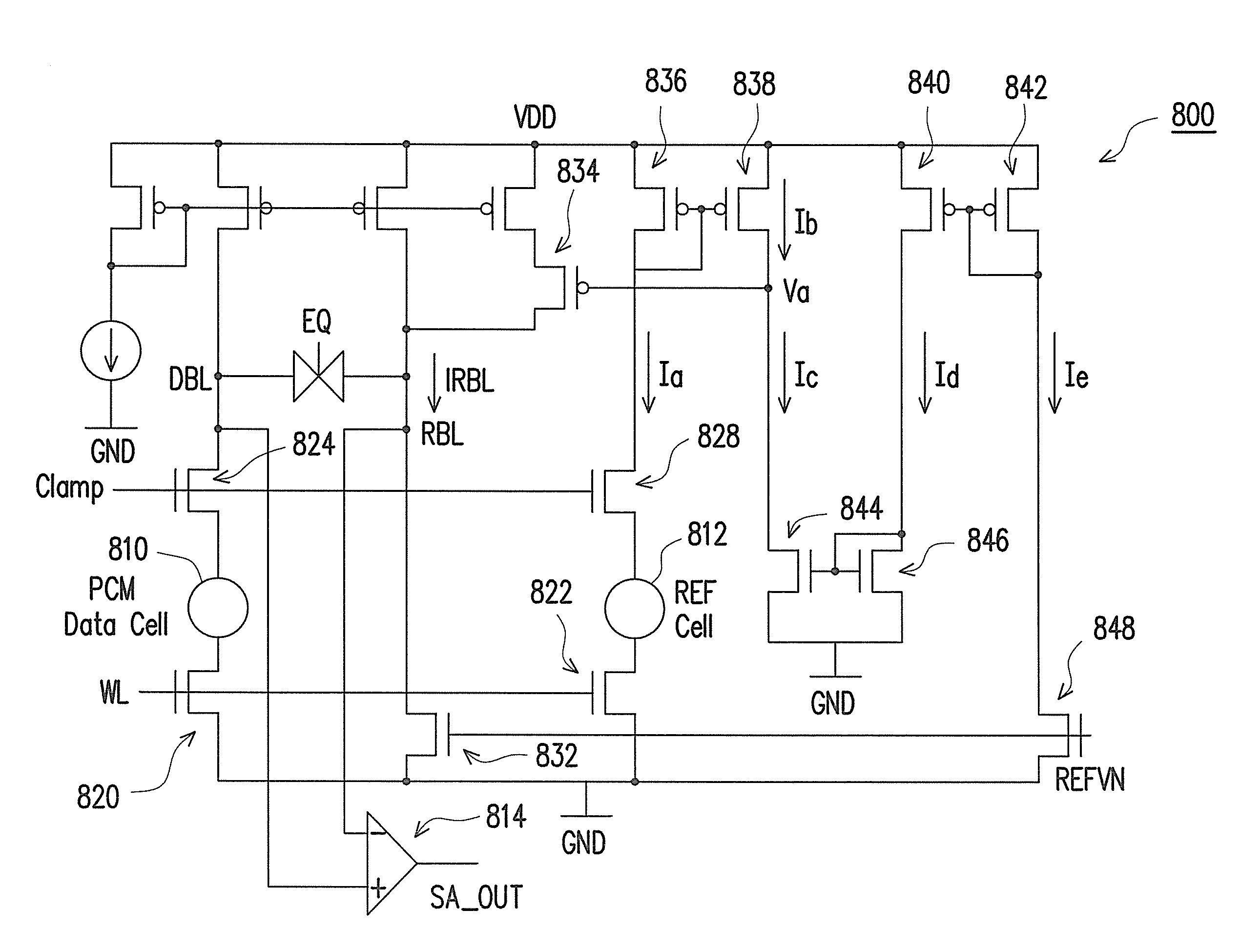
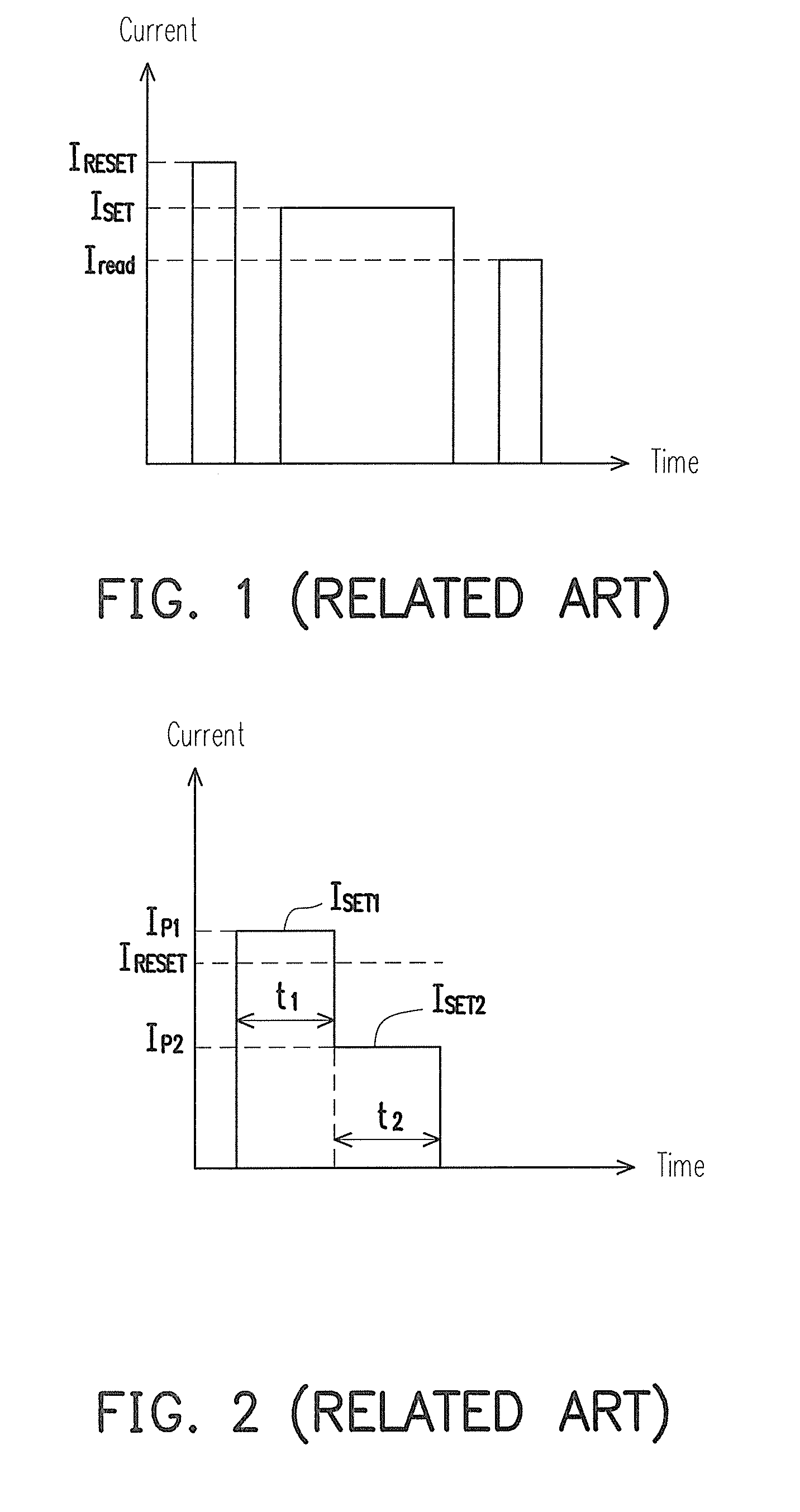
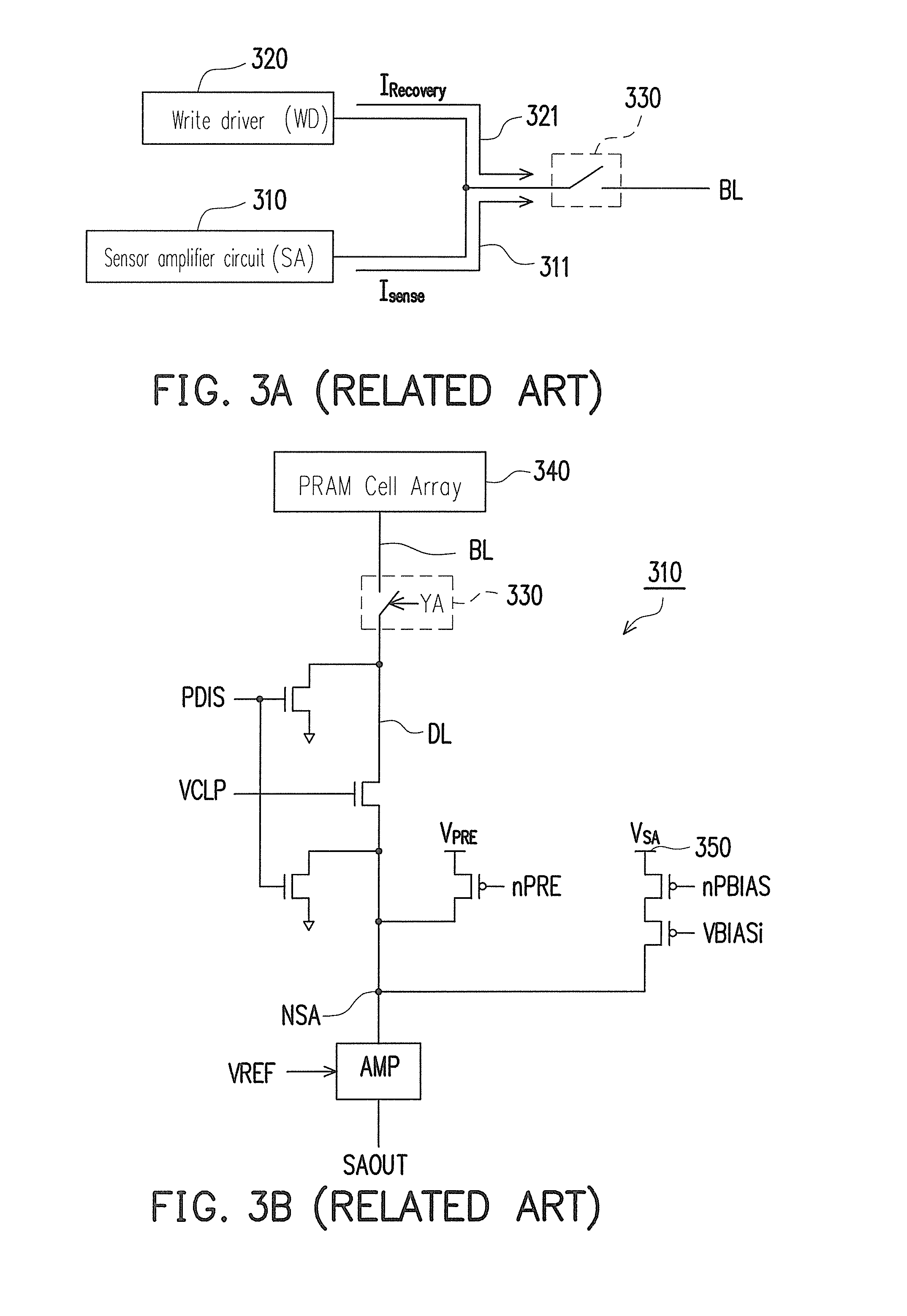
[0036]In one of exemplary embodiments, a memory device having a drift compensation function and an operation method thereof are introduced herein. If data stored in memory cell is not accessed for a long period of time, a resistance of the memory cell may be increased, and such characteristic may cause a problem of read error for a multi-level and high-impedance state read operation, for example, in one of exemplary embodiments, the read operation of a phase change memory (PCM) or a multi-level cell (MLC) flash memory, resistive random access memory (RRAM), etc. Therefore, a compensation mechanism may be required to resolve to resolve the problem of read error.

[0037]FIG. 7 is an operational schematic...


PUM


Abstract

A voltage compensation circuit, a multi-level memory device with the same, and a voltage compensation method for reading the multi-level memory device are provided. When a memory cell is read, a reference voltage applied to the memory device is adjusted according to variation of characteristics of a drift resistance of a reference cell. The increased value of the reference voltage (i.e. a voltage difference) corresponds to a resistance variation caused by a drift condition. The drift compensation mechanism is adaptive to a compensation circuit of a read driver of the memory device, which can compensate variation of the voltage level when data is read from the memory cell. When the resistance drift occurs, a drift amount is calculated and is added to the reference voltage, in order to avoid the error in judgement caused by the resistance drift when the stored data is read out.

Description

CROSS-REFERENCE TO RELATED APPLICATION[0001]This application claims the priority benefit of Taiwan application serial no. 98139567, filed on Nov. 20, 2009. The entirety of the above-mentioned patent application is hereby incorporated by reference herein and made a part of specification.BACKGROUND OF THE INVENTION[0002]1. Field of the Invention[0003]The present invention relates to a voltage compensation circuit, a multi-level memory device with the same, and a voltage compensation method for reading the multi-level memory device.[0004]2. Description of Related Art[0005]With development of portable electronic devices, demand for non-volatile memory is gradually increased. Since a phase change memory (PCM) technique has competitive characteristics of speed, power, capacity, reliability, process integration and cost, etc., it is regarded as a most promising next-generation non-volatile memory technique.[0006]Regarding an operation of the PCM, two different currents are applied to the P...

Claims


Application Information

Patent Timeline
IPC IPC(8): G11C7/00G11C11/00G11C5/14
CPCG11C7/14G11C11/5678G11C11/5685G11C13/0004G11C2211/5634G11C13/0038G11C13/004G11C13/0061G11C2013/0054G11C13/0007
Inventor SHEU, SHYH-SHYUANCHIANG, PEI-CHIALIN, WEN-PINLIN, CHIH-HE
Owner IND TECH RES INST
Why Eureka
Try Eureka