Stack type semiconductor package and method of fabricating the same

a semiconductor and stacking technology, applied in semiconductor devices, semiconductor/solid-state device details, electrical devices, etc., can solve the problem of difficult stacking of the upper semiconductor package on the lower semiconductor packag

Active Publication Date: 2012-07-05
SAMSUNG ELECTRONICS CO LTD
View PDF5 Cites 55 Cited by
  • Summary
  • Abstract
  • Description
  • Claims
  • Application Information

AI Technical Summary

Benefits of technology

[0006]One or more exemplary embodiments described herein provide a stack type semiconductor package in which an upper semiconductor package, including external connection terminals having fine pitches, is easily stacked on a lower semiconductor package, and a method of fabricating the stack type semiconductor package.

Problems solved by technology

If the pitches of external connection terminals of the upper semiconductor package of the stack type semiconductor package, i.e., the pitches of solder balls, are reduced and thus become fine, it is difficult to stack the upper semiconductor package on the lower semiconductor package.

Method used


Image

  • Stack type semiconductor package and method of fabricating the same
  • Stack type semiconductor package and method of fabricating the same
  • Stack type semiconductor package and method of fabricating the same

Examples


Embodiment Construction

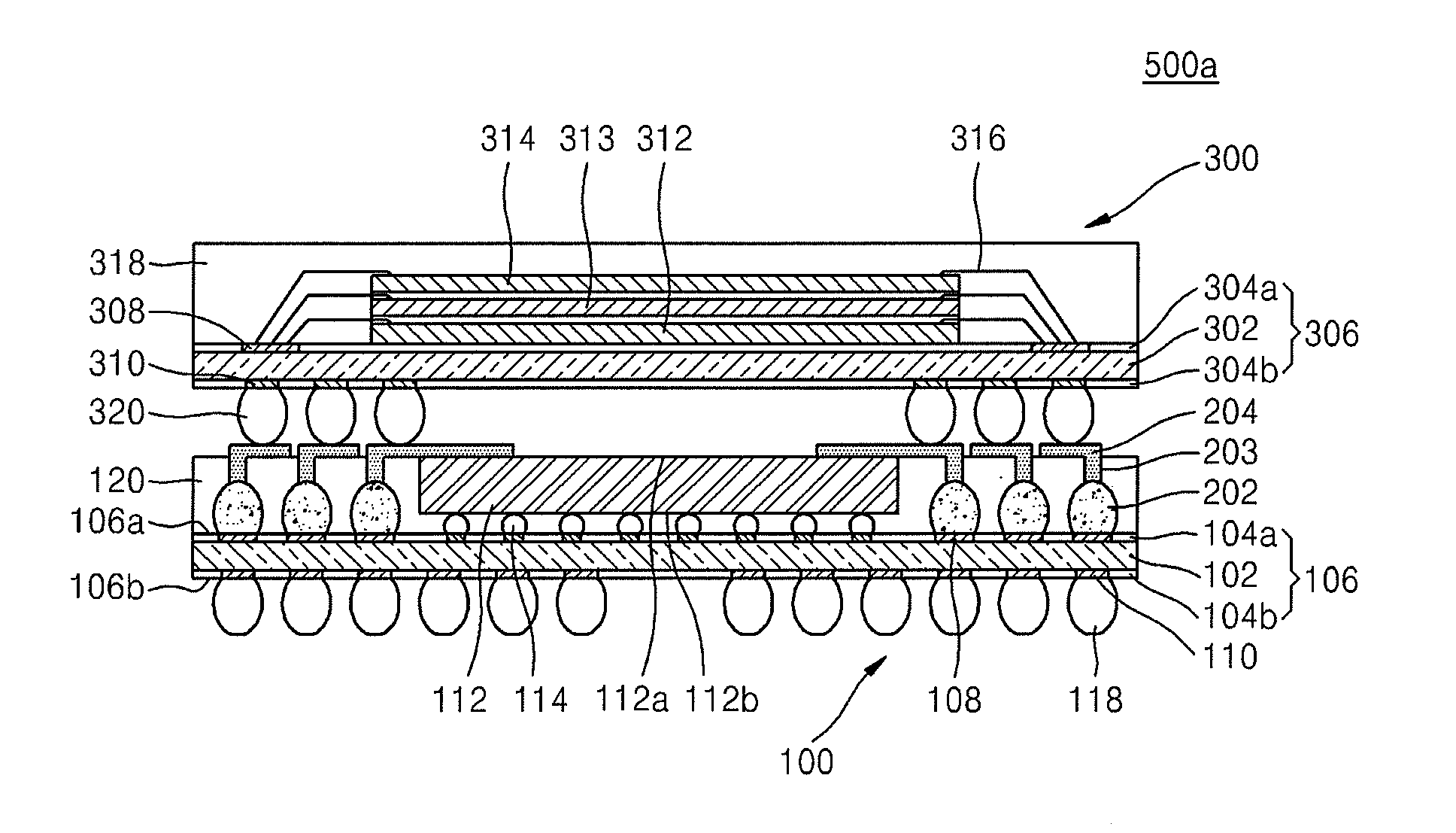
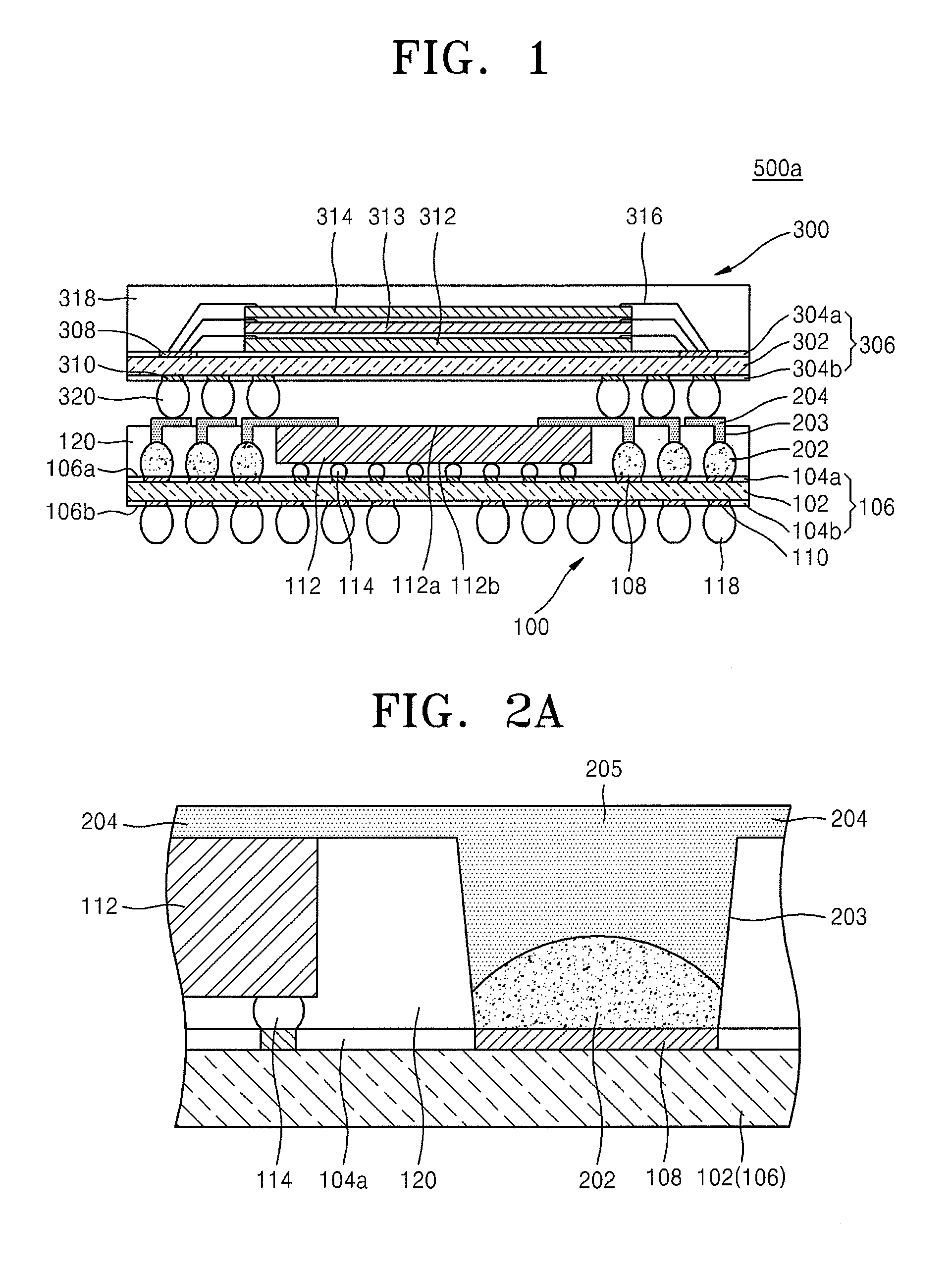
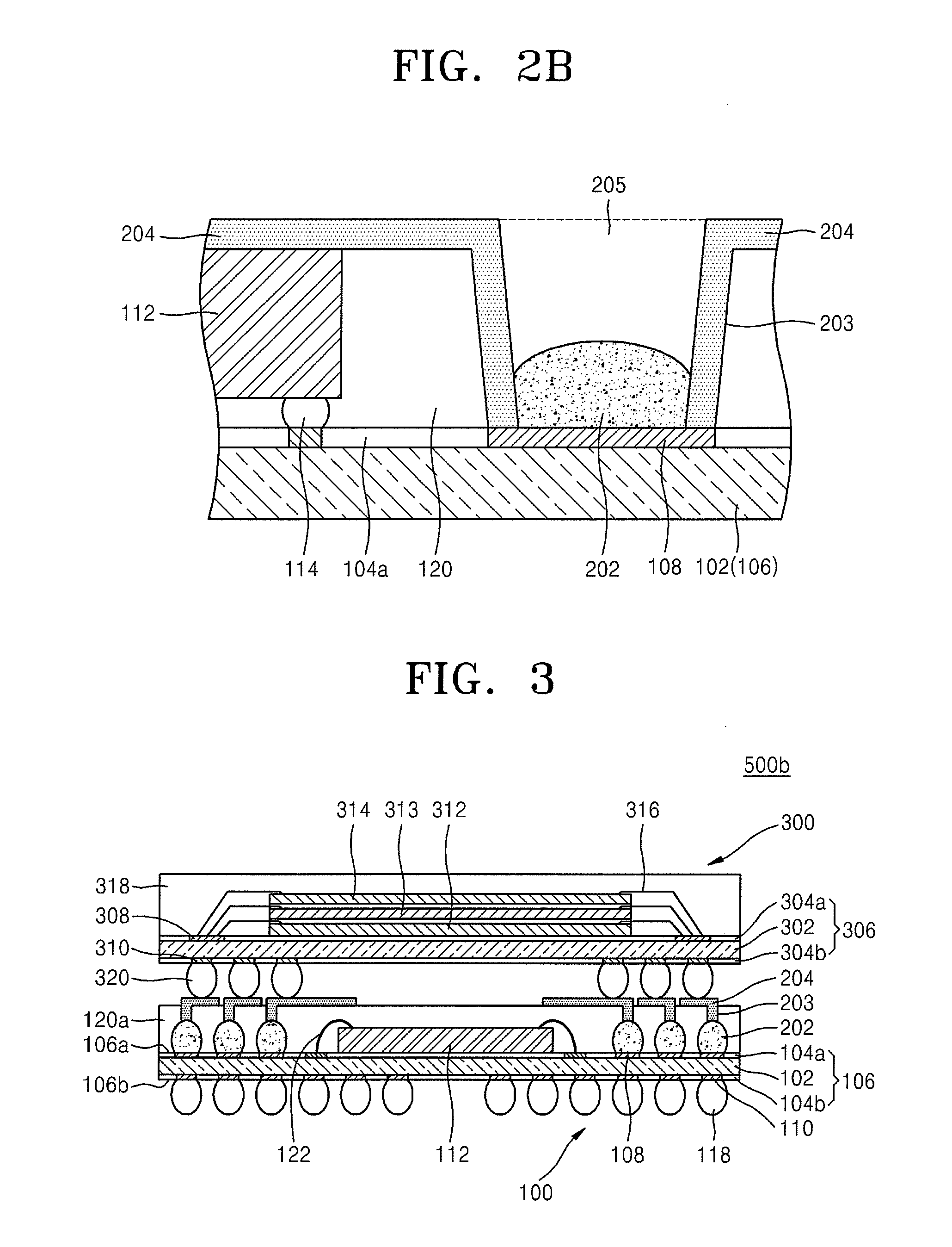
[0038]Exemplary embodiments will now be described more fully with reference to the accompanying drawings. The exemplary embodiments, however, should not be construed as being limited to the descriptions set forth herein. Like reference numerals in the drawings denote like elements, and thus their repeated description will be omitted. In the drawings, the thicknesses of layers and regions may be exaggerated for clarity.

[0039]The terminology used herein is for describing particular exemplary embodiments and is not intended to be limiting. As used herein, the singular forms “a,”“an,” and “the,” are intended to include the plural forms as well, unless the context clearly indicates otherwise. It will be further understood that the terms “comprises,”“comprising,”“includes,” and / or “including,” when used herein, specify the presence of stated features, integers, steps, operations, elements, and / or components, but do not preclude the presence or addition of one or more other features, integ...


PUM


Abstract

A stack type semiconductor package and a method of fabricating the stack type semiconductor package. The stack type semiconductor package includes: a lower semiconductor package including a circuit board, a semiconductor chip which is disposed on an upper surface of the circuit board, via-pads which are arrayed on the upper surface of the circuit board around the semiconductor chip, and an encapsulation layer which encapsulates the upper surface of the circuit board and has via-holes through which the via-pads are exposed; and an upper semiconductor package which is stacked on the encapsulation layer, is electrically connected to the lower semiconductor package, and comprises internal connection terminals which are formed on a lower surface of the upper semiconductor package.

Description

CROSS-REFERENCE TO RELATED APPLICATION[0001]This application claims priority from Korean Patent Application No. 10-2010-0140674, filed on Dec. 31, 2010, in the Korean Intellectual Property Office, the disclosure of which is incorporated herein in its entirety by reference.BACKGROUND[0002]1. Field[0003]Apparatuses and methods consistent with exemplary embodiments relate to a stack type semiconductor package and a method of fabricating the same, and more particularly, to a stack type semiconductor package in which a plurality of packages are stacked and a method of fabricating the same.[0004]2. Description of the Related Art[0005]A stack type semiconductor package is a package in which a plurality of semiconductor packages that have individually been packaged and electrically tested are vertically stacked. In a stack type semiconductor package, an upper semiconductor package should be stably stacked on a lower semiconductor package. If the pitches of external connection terminals of t...

Claims


Application Information

Patent Timeline
Patent Type & Authority Applications(United States)
IPC IPC(8): H01L23/495H01L23/48
CPCH01L23/3128H01L23/481H01L23/49816H01L23/49833H01L23/5389H01L24/24H01L24/82H01L25/105H01L2224/16227H01L2224/2402H01L2224/24051H01L2224/24105H01L2224/24226H01L2224/245H01L2224/48227H01L2224/73259H01L2224/73265H01L2224/82H01L2224/82105H01L2924/01029H01L2924/01082H01L24/48H01L2225/0651H01L2225/1023H01L2225/1041H01L2225/1058H01L2924/01033H01L2924/01047H01L2924/014H01L2924/15311H01L2924/18161H01L2225/06565H01L2224/16225H01L2224/32145H01L2224/32225H01L2924/1815H01L2924/00014H01L2924/00H01L2924/00012H01L2924/15322H01L24/73H01L2224/05008H01L2224/05573H01L2224/05001H01L2224/05569H01L2224/0558H01L2224/13025H01L2224/05572H01L2224/056H01L24/05H01L2224/8592H01L2224/45099H01L2224/45015H01L2924/207H01L23/12
Inventor YIM, CHOONG-BINCHOI, DAE-YOUNGKIM, MI-YEONPARK, JI-YONG
Owner SAMSUNG ELECTRONICS CO LTD
Why Eureka
Try Eureka