
IC tag reading and writing device, electronic apparatus, and IC tag reading and writing method

Inactive Publication Date: 2012-07-26
UEDA MASAHIDE
View PDF2 Cites 3 Cited by
  • Summary
  • Abstract
  • Description
  • Claims
  • Application Information

AI Technical Summary

Benefits of technology

[0011]An object of the invention is to provide an IC tag reading and writing device, an electronic apparatus, and an IC tag reading and writing method, capable of suppressing the influence on the antenna and circuit performing the communication with the IC tag in which the signal excited by the antennas which are not performing the communication with the IC tag have become a noise source.
[0017]According to the invention, it is possible to suppress the influence on the antenna and circuit performing the communication with the IC tag when the signal excited by the antennas which do not perform the communication with the IC tag have become a noise source.

Problems solved by technology

When the plurality of antennas are configured to be small in size and distances between the individual antennas are reduced, the signal excited in the antennas which do not perform the communication with the IC tag is a source of noise which may have an influence on the antenna and circuit performing the communication with the IC tag.

Method used


Image

  • IC tag reading and writing device, electronic apparatus, and IC tag reading and writing method
  • IC tag reading and writing device, electronic apparatus, and IC tag reading and writing method
  • IC tag reading and writing device, electronic apparatus, and IC tag reading and writing method

Examples


first embodiment

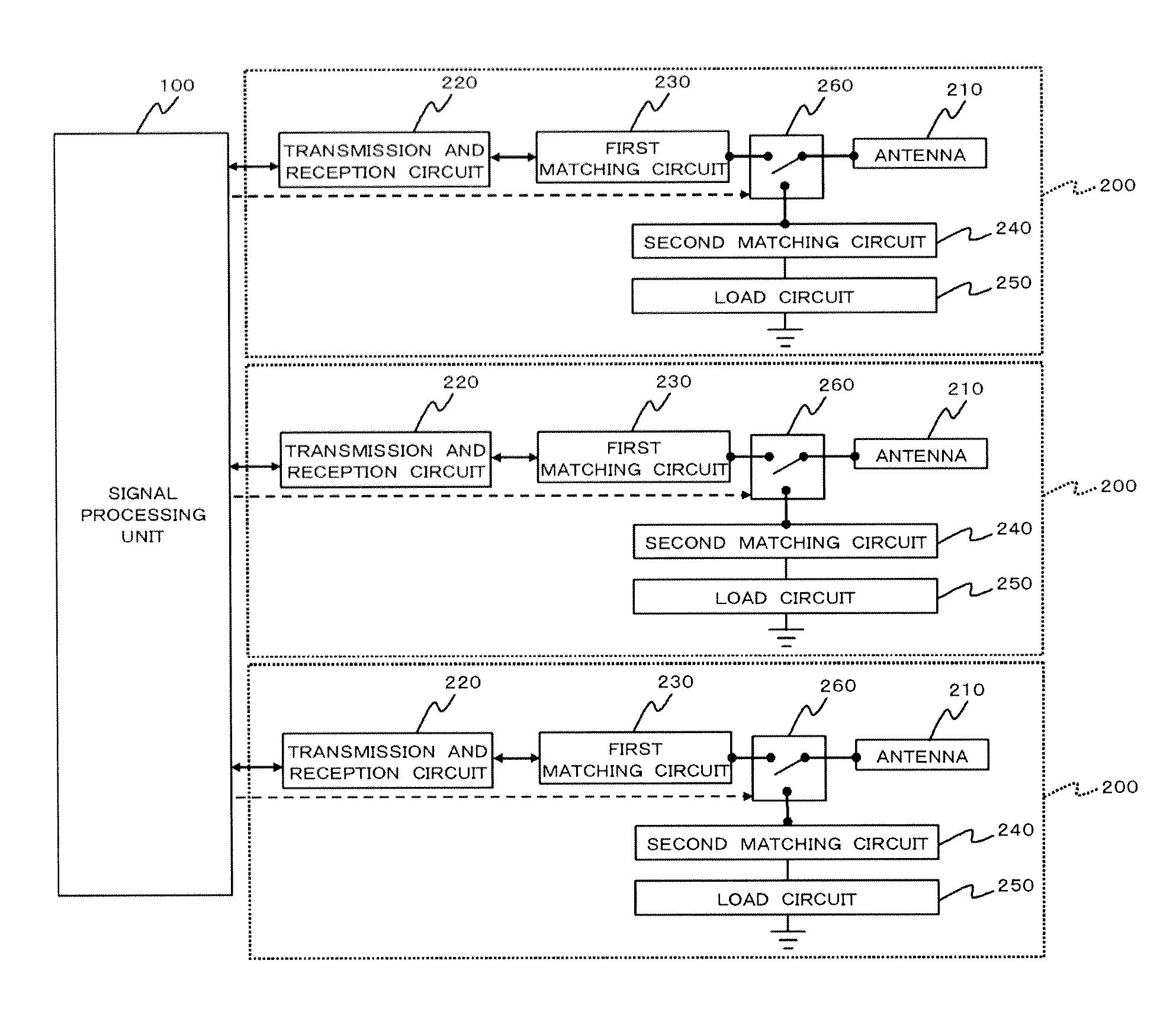
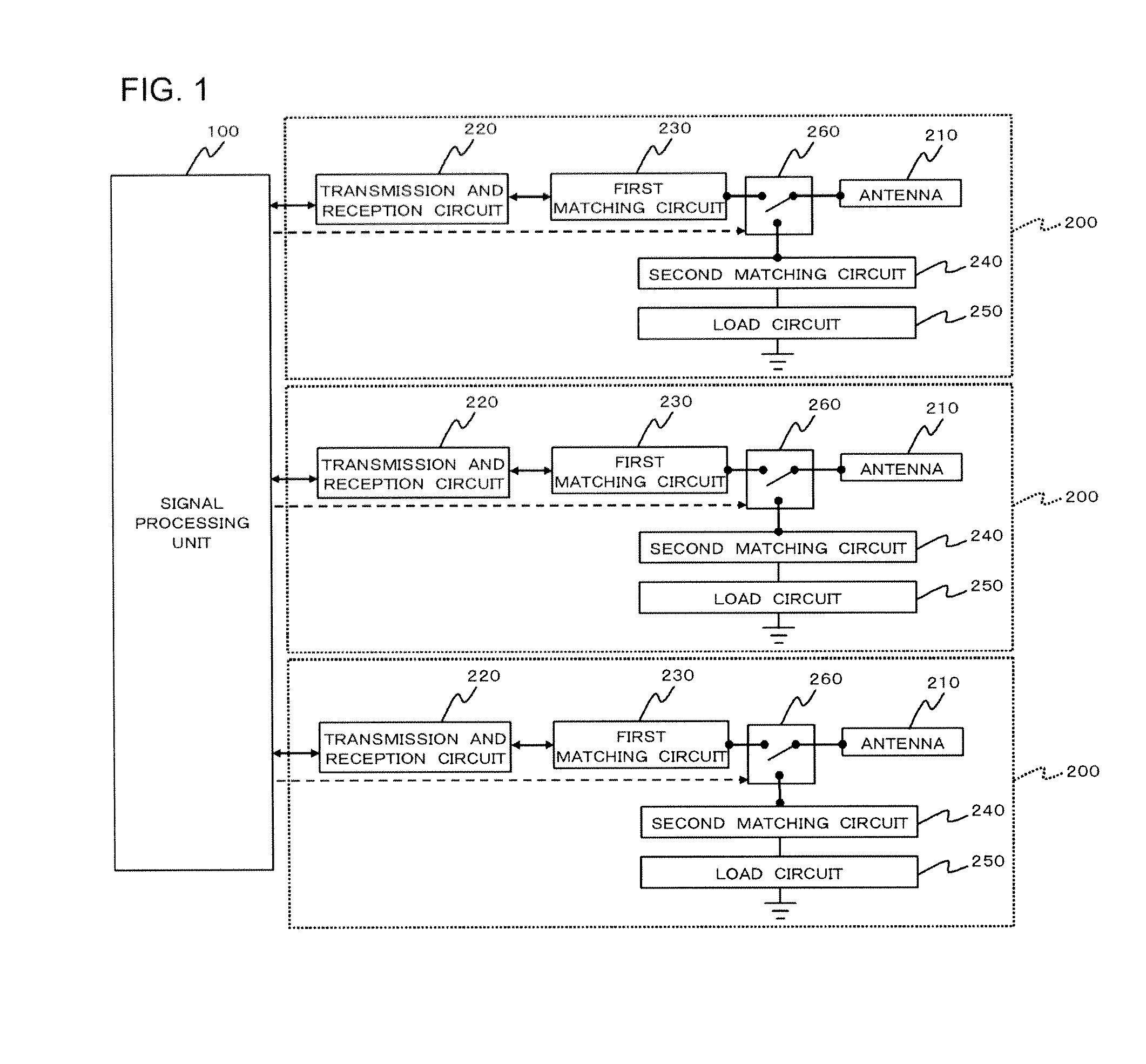
[0027]FIG. 1 is a block diagram illustrating a configuration of an IC tag reading and writing device according to a The IC tag reading and writing device is a device that performs communication with a plurality of kinds of IC tags over a plurality of communication frequencies, and is provided with a plurality of communication units 200 provided according to a plurality of frequencies, and a signal processing unit 100 that communicates with the plurality of kinds of IC tags through the plurality of communication units 200. Each of the plurality of communication units 200 is provided with an antenna 210, a transmission and reception circuit 220, a first matching circuit 230, a second matching circuit 240, and a switching unit 260. The first matching circuit 230 is connected to the transmission and reception circuit 220, and performs impedance matching between the antenna 210 and the transmission and reception circuit 220. The second matching circuit 240 is connected to a load circuit...

second embodiment

[0058]Also according to the embodiment, it is possible to obtain the same effect as that of the Although it is necessary to adjust the impedance of the second matching circuit 240 according to the impedance of the externally attached antenna 310, the adjustment may be performed by adjusting the capacitance value of the variable capacitor 242.

[0059]FIG. 7 is a block diagram illustrating a configuration of an IC tag reading and writing device according to a fifth embodiment. The reading and writing device has the same configuration as that of the IC tag reading and writing device according to anyone of the first to third embodiments, except that the signal processing unit 100 is externally attached to the electronic apparatus 12 formed of the plurality of communication units 200. In FIG. 7, the same configuration as the IC tag reading and writing device according to the third embodiment is shown. The electronic apparatus 12 is formed of, for example, one semiconductor chip.

[0060]Also...


PUM


Abstract

An object is to suppress an influence on an antenna and a circuit performing communication with an IC tag in which a signal excited by an antenna which does not perform communication with the IC tag is a noise source. When an IC tag reading and writing device performs communication with a first IC tag, the IC tag reading and writing device connects an antenna (210) to a first matching circuit (230) using a switching unit (260) in a communication unit (200) corresponding to a frequency of the first IC tag. In addition, the IC tag reading and writing device connects the antenna (210) to the second matching circuit (240) using the switching unit (260) in the other communication unit (200).

Description

[0001]The application claims priority based on Japanese Patent Application 2009-201885 filed Sep. 1, 2009, the entire of which is incorporated herein.TECHNICAL FIELD[0002]The present invention relates to an IC tag reading and writing device which performs reading and writing of a plurality of kinds of IC tags over a plurality of communication frequencies, an electronic apparatus, and an IC tag reading and writing method.BACKGROUND ART[0003]One kind of IC tag is the Radio Frequency Identification (RFID) tag. The RFID is characterized by having a low price, but there are a plurality of standards. Within the plurality of standards, the frequency bands for performing communication are not unified. To perform reading and writing of the plurality of kinds of RFIDs with different frequency bands, it is necessary to prepare a plurality of reading and writing devices based on the frequency bands and protocols thereof.[0004]In contrast, recently, the reading and writing of a plurality of kind...

Claims


Application Information

Patent Timeline
IPC IPC(8): G06K7/01
CPCG06K7/0008H04B5/00G06K7/10198
Inventor UEDA, MASAHIDE
Owner UEDA MASAHIDE
Learn More