Semiconductor apparatus and equipment

a technology of semiconductor and equipment, applied in the direction of electrical equipment, semiconductor devices, semiconductor/solid-state device details, etc., can solve the problems of metal pads corroding and high-density portions that can be excessively polished

Active Publication Date: 2021-04-08
CANON KK
View PDF0 Cites 0 Cited by
  • Summary
  • Abstract
  • Description
  • Claims
  • Application Information

AI Technical Summary

Benefits of technology

[0004]Some aspects of the present disclosure provide a technique for suppressing the communication of the internal space surrounded by two semiconductor components stacked on each other with the outside.

Problems solved by technology

When the face with the metal pads formed therein at an uneven density is polished by CMP, a high density portion can be excessively polished.
After stacking, when dicing the semiconductor components or forming an opening in the semiconductor component, if the internal space communicates with the outside, water or a foreign substance in the atmosphere may enter the internal space and the metal pads may corrode.

Method used


Image

  • Semiconductor apparatus and equipment
  • Semiconductor apparatus and equipment
  • Semiconductor apparatus and equipment

Examples


first embodiment

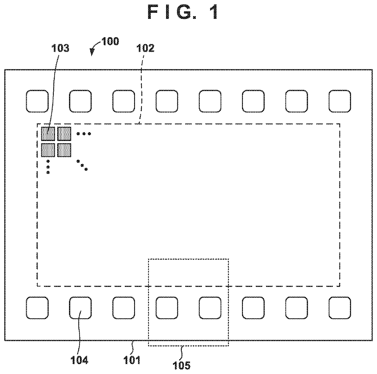
[0017]With reference to FIG. 1, an example of the structure of a semiconductor apparatus 100 according to the first embodiment of the present disclosure will be described. FIG. 1 is a plan view of the semiconductor apparatus 100. FIG. 1 shows a photoelectric conversion apparatus (for example, a solid-state imaging apparatus) as an example of the semiconductor apparatus 100. The semiconductor apparatus 100 includes, in its center, a pixel region 102 in which a plurality of pixels 103 are arranged in a two-dimensional array. Each pixel 103 may include, for example, a photoelectric conversion element such as a photodiode, and a switch element such as a transistor.

[0018]The semiconductor apparatus 100 further includes a plurality of openings 104. In FIG. 1, only one opening 104 is given a reference numeral, but all the 16 elements having the same shape as the opening 104 are the openings 104. As will be described later, the opening 104 exposes the bonding pad of the semiconductor appara...

second embodiment

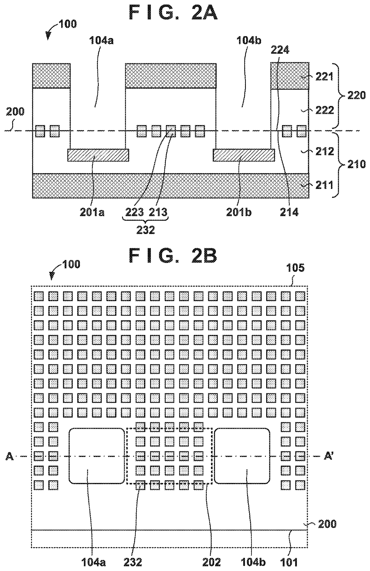
[0048]With reference to FIGS. 6A and 6B, an example of the structure of a semiconductor apparatus 600 according to the second embodiment of the present disclosure will be described. A repetitive description of components of the semiconductor apparatus 600 similar to those of the semiconductor apparatus 100 will be omitted. That is, unless otherwise stated, the above description of the semiconductor apparatus 100 also applies to the semiconductor apparatus 600.

[0049]FIG. 6A is a sectional view of the semiconductor apparatus 600 in the region 105 shown in FIG. 1. FIG. 6B shows the structure of the semiconductor apparatus 600 on a bonding face 200 between a semiconductor component 210 and a semiconductor component 220. FIG. 6A is a sectional view taken along a line B-B′ in FIG. 6B.

[0050]A plurality of bonding portions 232 are arranged over the entire bonding face 200. For example, some of the plurality of bonding portions 232 are arranged in a region overlapping with the pixel region 1...

third embodiment

[0062]With reference to FIG. 8, an example of the structure of a semiconductor apparatus 800 according to the third embodiment of the present disclosure will be described. A repetitive description of components of the semiconductor apparatus 800 similar to those of the semiconductor apparatus 100 or 600 will be omitted. That is, unless otherwise stated, the above description of the semiconductor apparatus 100 or 600 also applies to the semiconductor apparatus 800.

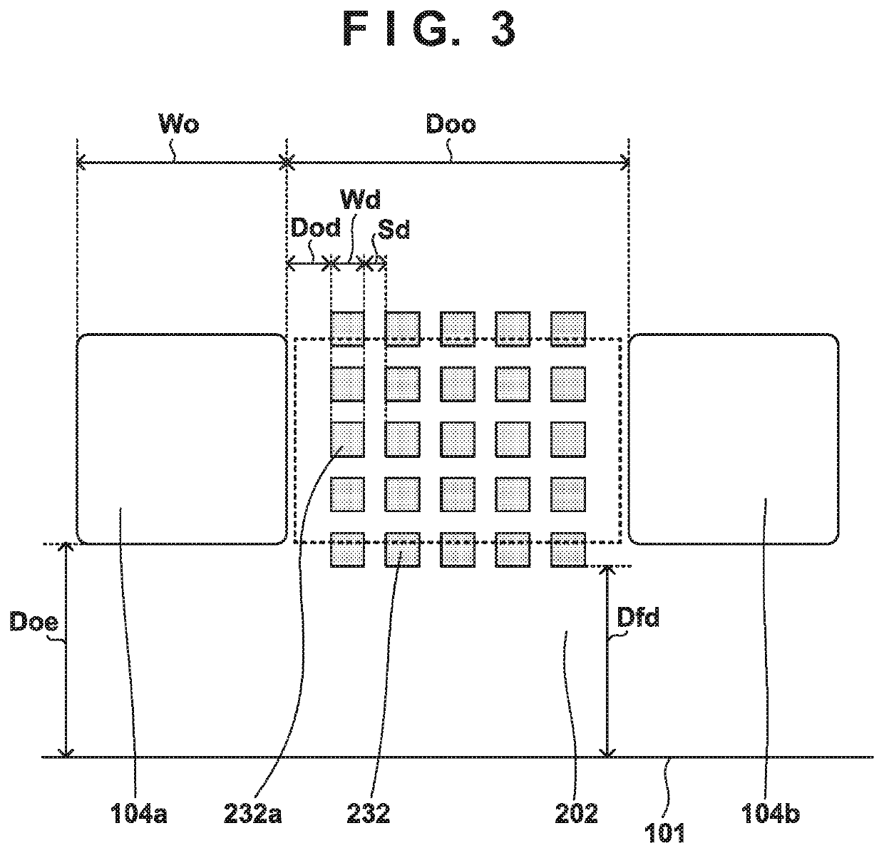
[0063]FIG. 8 shows the structure of the semiconductor apparatus 800 in the region 105 shown in FIG. 1 on a bonding face 200 between a semiconductor component 210 and a semiconductor component 220. A plurality of bonding portions232 are arranged over the entire bonding face 200. For example, some of the plurality of bonding portions 232 are arranged in a region overlapping with the pixel region 102. Further, some of the plurality of bonding portions 232 are arranged in a region 202 between an opening 104a and an opening 104b...


PUM

PropertyMeasurementUnit
angleaaaaaaaaaa
angleaaaaaaaaaa
angleaaaaaaaaaa

Abstract

A semiconductor apparatus includes included first and second semiconductor components which are stacked on each other. The first component includes a first insulating layer and a first plurality of metal pads. The second component includes a second insulating layer and a second plurality of metal pads. Each of the first plurality of metal pads and each of the second plurality of metal pads are bonded to each other to form each of a plurality of bonding portions. First and second openings along an edge of the apparatus and passing through a bonding face between the first and second insulating layer are formed in the apparatus. A first bonding portion between the first opening and the second opening of the plurality of bonding portions is arranged in a distinctive location.

Description

BACKGROUND OF THE INVENTIONField of the Invention[0001]The present disclosure relates to a semiconductor apparatus and an equipment.Description of the Related Art[0002]Japanese Patent Laid-Open No. 2017-120939 describes that a semiconductor apparatus having a three-dimensional structure is formed by stacking two semiconductor components each including elements and a wiring structure. In this semiconductor apparatus, electrodes are formed in the respective bonding faces of the two semiconductor components, and the elements of the two semiconductor components are electrically connected by bonding the electrodes.[0003]Metal pads in the bonding face of the semiconductor component can be formed using a wiring forming technique generally known as a damascene method. For example, the metal pads are formed by forming grooves in an insulating layer that forms the bonding face of the semiconductor component, performing copper plating from above the grooves, and removing the copper other than ...

Claims


Application Information

Patent Timeline
Patent Type & Authority Applications(United States)
IPC IPC(8): H01L23/00H01L25/065H01L25/16H01L25/18
CPCH01L24/06H01L25/0657H01L25/167H01L2224/80948H01L24/80H01L24/03H01L2224/06102H01L25/18H01L27/14636H01L2224/09517H01L2224/80895H01L2224/80896H01L2224/80986H01L2224/03616H01L2224/08145H01L25/50H01L2224/05647H01L2224/05624H01L2224/05684H01L2224/73201H01L2224/04042H01L2224/0346H01L2224/0345H01L2224/0807H01L2224/08057H01L23/564H01L2224/0603H01L2224/05554H01L2224/06132H01L2224/06134H01L24/08H01L2924/10155H01L24/48H01L2924/00014H01L2224/08H01L2224/48
Inventor OGAWA, TOSHIYUKI
Owner CANON KK
Why Eureka
Try Eureka