
Semiconductor charge storage apparatus and methods

a technology of charge storage and semiconductor devices, applied in the direction of electrical devices, semiconductor devices, nanotechnology, etc., can solve the problem that multi-tiered semiconductor devices can be expensive to fabrica

Active Publication Date: 2012-08-30
MICRON TECH INC
View PDF1 Cites 77 Cited by
  • Summary
  • Abstract
  • Description
  • Claims
  • Application Information

AI Technical Summary

Problems solved by technology

Multi-tiered semiconductor devices can be expensive to fabricate because it is difficult to form features in multiple tiers of semiconductor material.

Method used


Image

  • Semiconductor charge storage apparatus and methods
  • Semiconductor charge storage apparatus and methods
  • Semiconductor charge storage apparatus and methods

Examples


Embodiment Construction

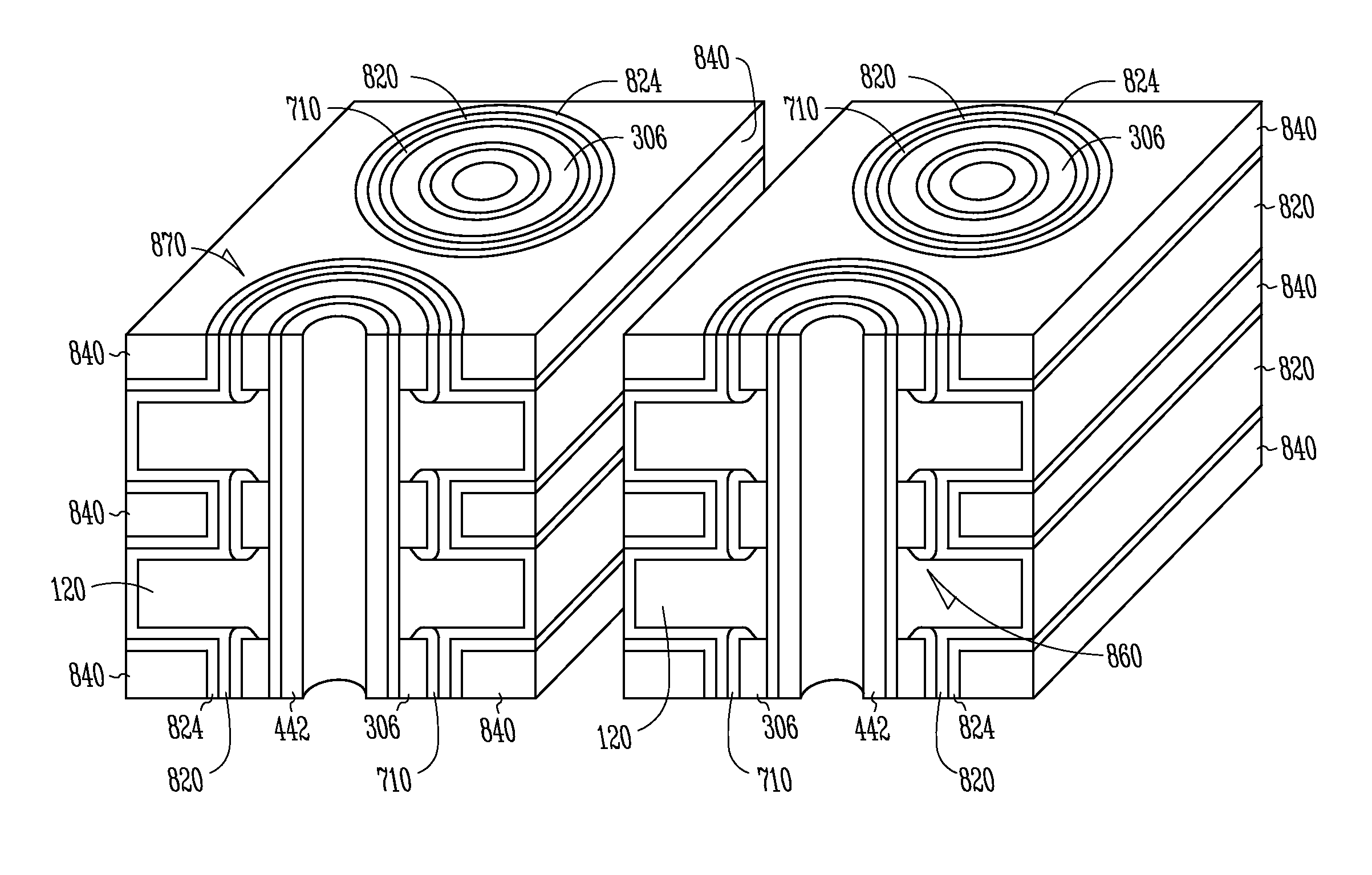
[0024]An array of charge storage devices according to various embodiments of the invention may function as an array of memory cells in a memory device such as a NOT AND (NAND) memory device.

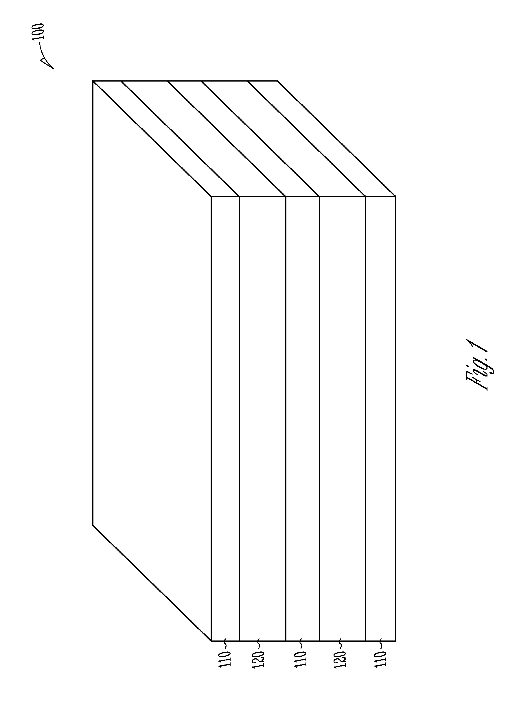
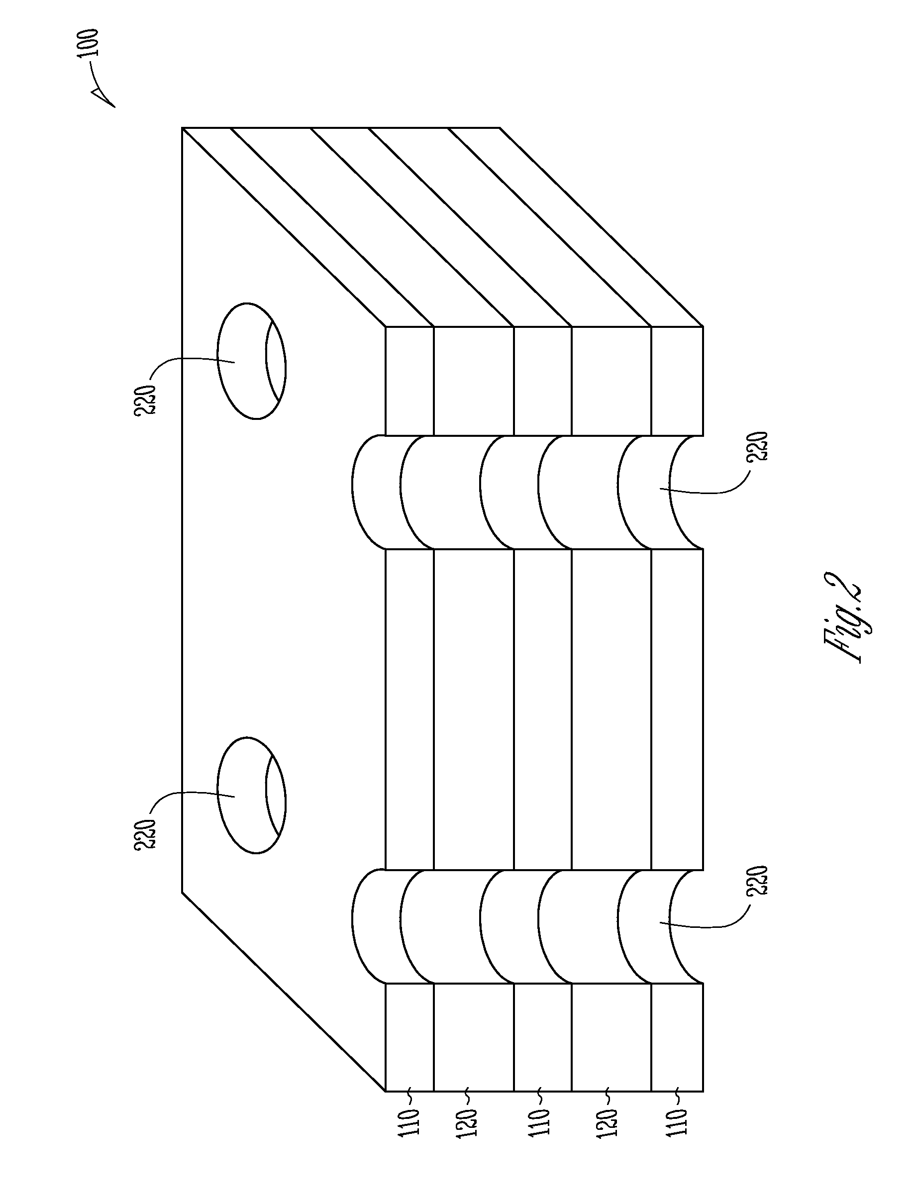
[0025]FIG. 1 is a three-dimensional view of a semiconductor construction 100 according to various embodiments of the invention. Tiers and regions in the semiconductor construction 100 will be identified by the same reference numerals throughout FIGS. 1-8 for purposes of brevity and clarity. An array of charge storage devices comprising thin film transistors (TFT) are to be formed in the semiconductor construction 100 as will be described herein below. The semiconductor construction 100 comprises an array of NAND strings of memory cells according to various embodiments of the invention.

[0026]The semiconductor construction 100 includes alternating tiers of a semiconductor material such as undoped polysilicon 110 and a dielectric 120. Each tier of dielectric 120 is between, and in contact with, two ...


PUM


Abstract

Methods of forming multi-tiered semiconductor devices are described, along with apparatus and systems that include them. In one such method, an opening is formed in a tier of semiconductor material and a tier of dielectric. A portion of the tier of semiconductor material exposed by the opening is processed so that the portion is doped differently than the remaining semiconductor material in the tier. At least substantially all of the remaining semiconductor material of the tier is removed, leaving the differently doped portion of the tier of semiconductor material as a charge storage structure. A tunneling dielectric is formed on a first surface of the charge storage structure and an an intergate dielectric is formed on a second surface of the charge storage structure. Additional embodiments are also described.

Description

BACKGROUND[0001]Non-volatile semiconductor memories (NVSMs) are widely used in many electronic devices such as personal digital assistants (PDAs), laptop computers, mobile phones and digital cameras. Some of these memories have arrays of charge storage transistors, such as floating gate transistors.BRIEF DESCRIPTION OF THE DRAWINGS[0002]Some embodiments are illustrated by way of example and not limitation in the figures of the accompanying drawings in which:[0003]FIG. 1 is a three-dimensional view of a semiconductor construction according to various embodiments of the invention;[0004]FIG. 2 is a three-dimensional view of a semiconductor construction according to various embodiments of the invention;[0005]FIG. 3 is a three-dimensional view of a semiconductor construction according to various embodiments of the invention;[0006]FIG. 4 is a three-dimensional view of a semiconductor construction according to various embodiments of the invention;[0007]FIG. 5 is a three-dimensional view of...

Claims


Application Information

Patent Timeline
IPC IPC(8): H01L29/78H01L21/28H01L21/336B82Y99/00
CPCH01L27/11524H01L29/7926H01L27/11556H01L29/7889H01L29/40114H10B41/35H10B41/27H01L21/823487H01L29/792H01L29/40117H10B41/30H10B43/20H10B43/27H01L29/04H01L29/167H01L29/495H01L29/4966
Inventor TANG, SANH D.ZAHURAK, JOHN K.
Owner MICRON TECH INC
Features
  • Generate Ideas
  • Intellectual Property
  • Life Sciences
  • Materials
  • Tech Scout
  • Unparalleled Data Quality
  • Higher Quality Content
  • 60% Fewer Hallucinations
Learn More