Single-to-differential conversion circuit

a conversion circuit and single-to-differential technology, applied in the direction of pulse manipulation, pulse technique, inductance, etc., can solve problems such as unbalanced set of differential signals

Active Publication Date: 2012-10-04
REALTEK SEMICON CORP
View PDF2 Cites 12 Cited by
  • Summary
  • Abstract
  • Description
  • Claims
  • Application Information

AI Technical Summary

Benefits of technology

[0011]Therefore, an object of the present invention is to provide a single-to-differential conversion circuit with gain compensation.
[0011]Therefore, an object of the present invention is to provide a single-to-differential conversion circuit with gain compensation.

Problems solved by technology

The gain mismatch of the first and second differential voltages Vo1, Vo2 in the set of differential signals will result in unbalanced set of differential signals.

Method used


Image

  • Single-to-differential conversion circuit
  • Single-to-differential conversion circuit
  • Single-to-differential conversion circuit

Examples


Embodiment Construction

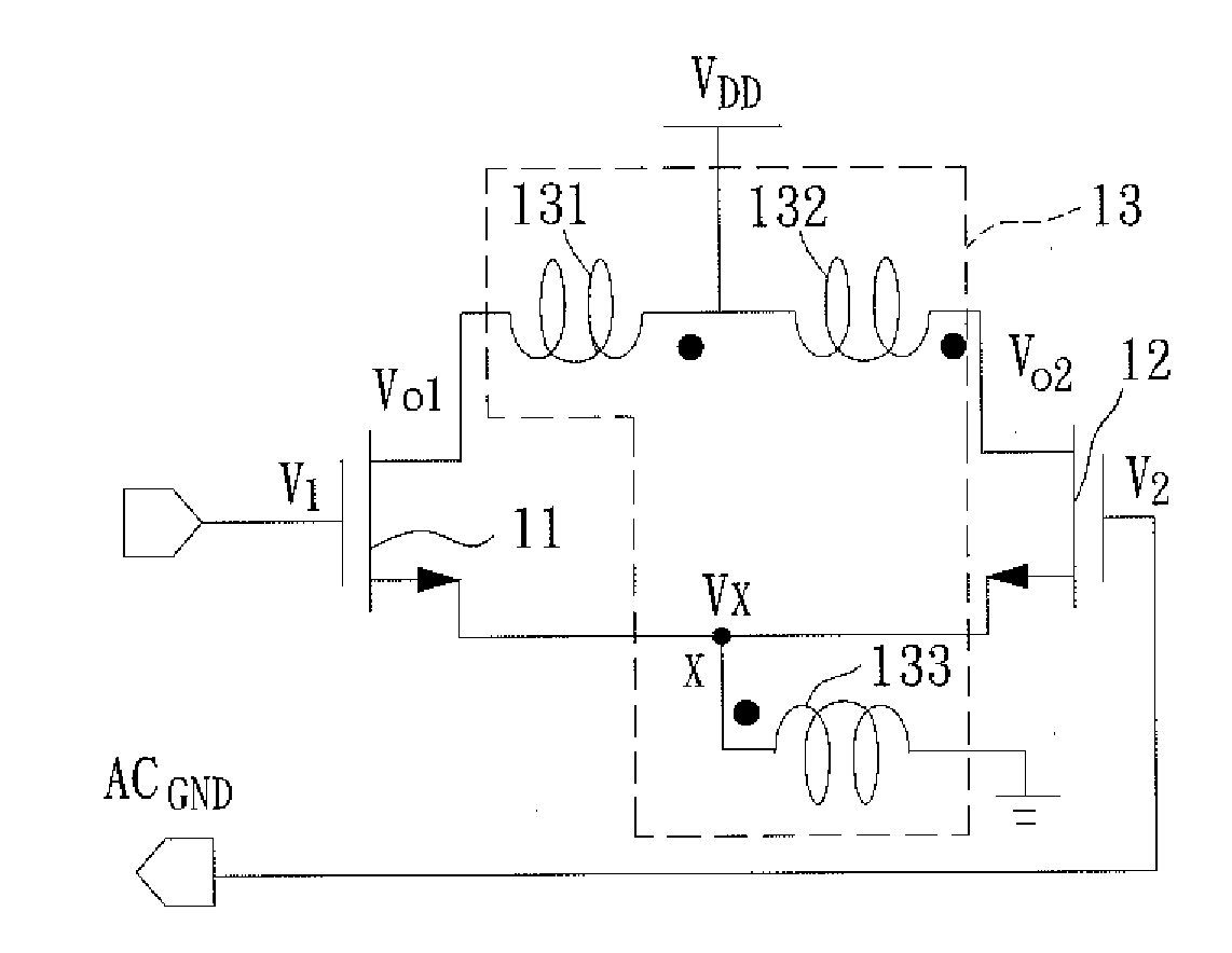
[0023]FIG. 3 shows the preferred embodiment of a single-to-differential conversion circuit of the present invention that comprises a first transistor 11, a second transistor 12, and a transforming unit 13.

[0024]The first transistor 11 has a first terminal, a second terminal, and a third terminal which receives an input signal. The second transistor 12 has a first terminal, a second terminal and a third terminal. In the present embodiment, the first and second transistors 11, 12 are both N-type metal oxide semiconductor-field effect transistors. The first terminals of both first and second transistors 11, 12 are source terminals. The second terminals of both first and second transistors 11, 12 are drain terminals. The third terminals of both first and second transistors 11, 12 are gate terminals.

[0025]The transforming unit 13 has a first induction element 131, a second induction element 132 and a third induction element 133. The first induction element 131 has a first inductive termi...


PUM


Abstract

A single-to-differential conversion circuit includes a first transistor, a second transistor, and a transforming unit. Each of the first and second transistors has first, second and third terminals. The trans forming unit has first, second, and third induction elements. The first induction element has a first inductive terminal coupled to the second terminal of the first transistor, and a second inductive terminal coupled to a voltage source. The second induction element has a first inductive terminal to be coupled to the voltage source, and a second inductive terminal coupled to the second terminal of the second transistor. The third induction element has a first inductive terminal coupled to the first terminals of the first and second transistors, and a second inductive terminal coupled to ground. The third induction element electrically couples to the first and the second induction elements according to first and second coupling parameters, respectively.

Description

CROSS-REFERENCE TO RELATED APPLICATION[0001]This application claims priority to Taiwanese Patent Application No. 100111572, filed on Apr. 1, 2011, the disclosure of which is incorporated herein by reference.BACKGROUND OF THE INVENTION[0002]1. Field of the Invention[0003]The invention relates to a single-to-differential conversion circuit, more particularly to a single-to-differential conversion circuit with gain compensation.[0004]2. Description of the Related Art[0005]In a telecommunication system, the receiver usually needs to use a single-to-differential conversion circuit to convert a received radio frequency (RF) signal into a differential signal having a first differential voltage and a second differential voltage. Under ideal conditions, the first and second differential voltages should be the same in magnitude, and 180° out of phase.[0006]Looking at the current technology of the related circuit and the small signal model for a single-to-differential conversion circuit as sho...

Claims


Application Information

Patent Timeline
Patent Type & Authority Applications(United States)
IPC IPC(8): H03K5/00
CPCH01L28/10H04L25/0272H03K19/018528H03K19/018521
Inventor CHEN, HSIEN-KU
Owner REALTEK SEMICON CORP
Why Eureka
Try Eureka