Protective element for electronic circuits

a protection element and electronic circuit technology, applied in the direction of basic electric elements, electrical apparatus, semiconductor devices, etc., can solve the problems of restricting their use at elevated temperatures, and achieve the effects of avoiding or reducing the occurring power loss or voltage, and reducing the amount of voltage drop via the protective elemen

Active Publication Date: 2012-11-08
ROBERT BOSCH GMBH
View PDF6 Cites 0 Cited by
  • Summary
  • Abstract
  • Description
  • Claims
  • Application Information

AI Technical Summary

Benefits of technology

[0006]The device according to the present invention and the method according to the present invention have the advantage that the above-mentioned disadvantages no longer occur. To avoid or decrease the occurring power loss or the voltage, a system is used in which diode D is replaced by a Schottky diode S. Due to the lower forward voltage of a Schottky diode, the voltage drop via the protective element is less. However, relatively high leakage or reverse currents occur in Schottky diodes, which restrict their use at elevated temperatures. Since the forward voltages of a Schottky diode are generally lower than in pn-diodes, their reverse currents are also higher. In addition, the reverse current of a simple Schottky diode increases with increasing reverse voltage.

Problems solved by technology

However, relatively high leakage or reverse currents occur in Schottky diodes, which restrict their use at elevated temperatures.

Method used


Image

  • Protective element for electronic circuits
  • Protective element for electronic circuits
  • Protective element for electronic circuits

Examples


Embodiment Construction

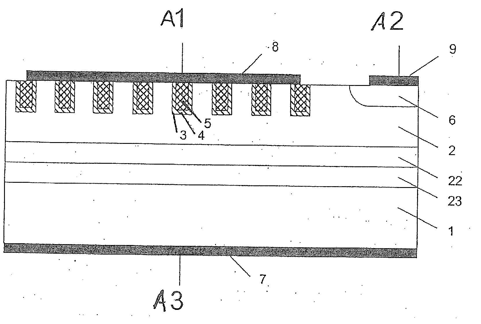
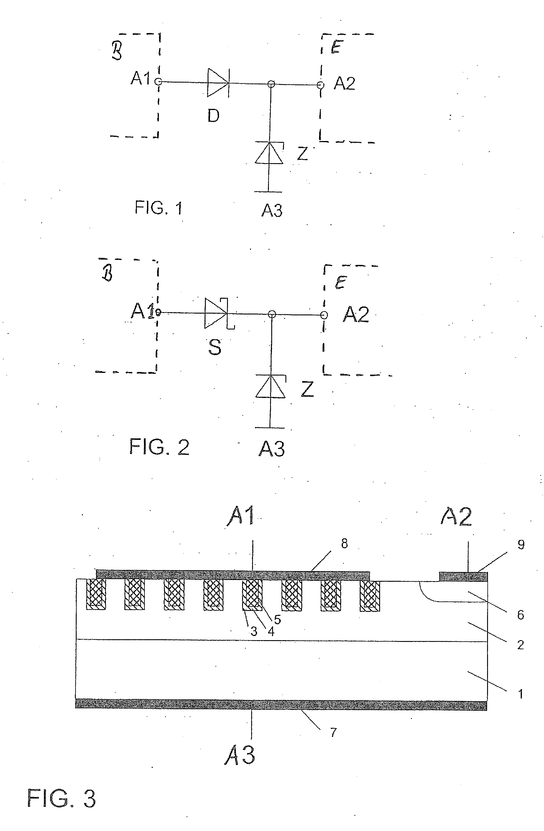
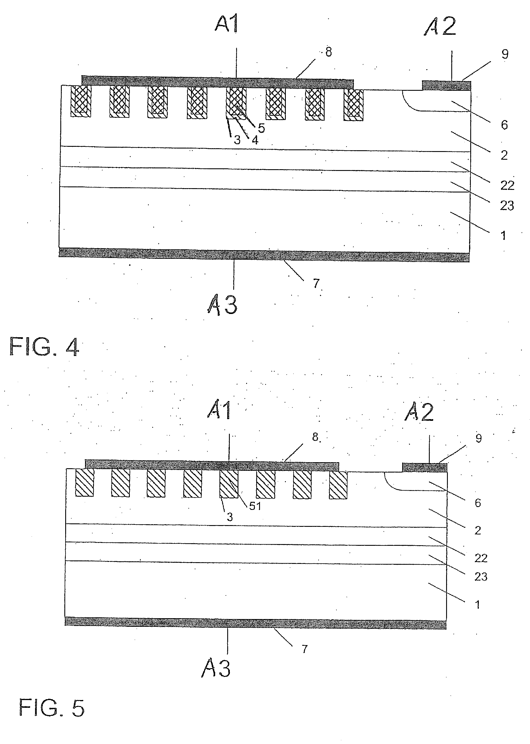
[0012]FIG. 2 shows a circuit diagram of a protective element or a protective system according to the present invention having Schottky diode S instead of pn-diode and Z or Zener diode Z. In this protective system, which may also be integrated into a semiconductor, a Schottky diode S is thus used as the polarity reversal protection diode and a Z diode Z is used for the overvoltage protection. The protective system is connected between the power supply, i.e., the battery or accumulator, and the electronics. Terminal Al is connected to the voltage supply and terminal A2 is connected to the electronics. A3 is connected to ground.

[0013]A Schottky diode or Schottky diodes may also be used, in the case of which the voltage-dependent fraction of the reverse current may be substantially suppressed. Examples thereof are TMBS diodes (trench MOS barrier junction diodes) or TJBS diodes (trench junction barrier Schottky diodes).

[0014]Furthermore, Schottky diodes S in a protective system according...


PUM


Abstract

A protective element for electronics has at least one Schottky diode and at least one Zener diode which are located between a power supply and the electronics, the anode of the Schottky diode being connected to the power supply and the cathode of the Schottky diode being connected to the electronics, and the cathode and the anode of the Zener diode are connected to ground. The Schottky diode is a trench MOS barrier junction diode or trench MOS barrier Schottky (TMBS) diode or a trench junction barrier Schottky (TJBS) diode and includes an integrated semiconductor arrangement, which has at least one trench MOS barrier Schottky diode and a p-doped substrate, which is used as the anode of the Zener diode.

Description

BACKGROUND OF THE INVENTION[0001]1. Field of the Invention[0002]The present invention relates to a protective element for electronic circuits.[0003]2. Description of Related Art[0004]Many electronic circuits and components are supplied with power from a battery or an accumulator. In many applications, it is possible that the battery or the accumulator may be connected to the electronic circuit with incorrect polarity. In this case, the positive pole of the battery is unintentionally applied to the negative terminal of the circuit and the negative pole is applied to the positive terminal. This procedure is referred to as polarity reversal. For example, the accumulator of a motor vehicle may unintentionally be connected the wrong way around in the event of maintenance or repair work. High currents may thus flow through the connected electronic circuits and damage them. A pn-diode, which is inserted between the accumulator and the electronic circuit, may be used as a corrective measure...

Claims


Application Information

Patent Timeline
Patent Type & Authority Applications(United States)
IPC IPC(8): H01L29/47H01L21/20
CPCH01L27/0248H01L29/8725H01L29/872H01L29/866
Inventor QU, NINGGOERLACH, ALFRED
Owner ROBERT BOSCH GMBH
Why Eureka
Try Eureka