Method for manufacturing semiconductor device, resin sealing apparatus, and semiconductor device

Inactive Publication Date: 2013-01-24
ASAHI ENG CO LTD
View PDF3 Cites 3 Cited by
  • Summary
  • Abstract
  • Description
  • Claims
  • Application Information

AI Technical Summary

Benefits of technology

The present invention provides a method for manufacturing a semiconductor device with a cavity inside a seal glass while protecting the seal glass with a release film. The method prevents bending stress on the seal glass and breakage of the seal glass due to bending. A film escape recess is formed at the mold die to allow an escape of the release film pressure, reducing increases in the size and cost of the semiconductor device. The semiconductor device is clamped by the mold die at a pressure capable of preventing generation of a thin flash while preventing breakage of the seal glass. The film escape area is formed at the mold die or the seal glass, reducing the size and cost of the semiconductor device.

Problems solved by technology

However, the method discussed in PTL 1 requires the support frame to be disposed around the seal glass, thereby requiring preparation of a space therefore, leading to the possibility of an increase in the size of the semiconductor device.
Further, the necessity of additional cost for the provision of the support frame and an additional process for mounting the support frame may result in an increase in the manufacturing cost of the semiconductor device.

Method used


Image

  • Method for manufacturing semiconductor device, resin sealing apparatus, and semiconductor device
  • Method for manufacturing semiconductor device, resin sealing apparatus, and semiconductor device
  • Method for manufacturing semiconductor device, resin sealing apparatus, and semiconductor device

Examples


first embodiment

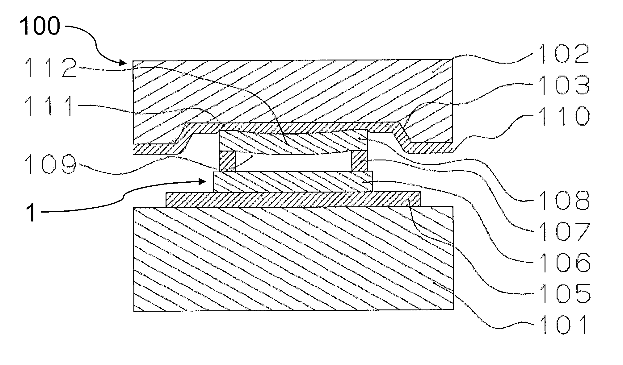
[0029]To achieve the above-described object, a method for manufacturing a semiconductor device according to an embodiment of the present invention is characterized in that a film escape recess is formed at a cavity of an upper die, thereby preventing generation of a bending stress at a portion of a seal glass below which there is a cavity, due to a pressure of a release film. A reason for breakage of the seal glass is that a bending stress is generated at the seal glass by a pressure generated when the film is pressed against the central portion of the seal glass due to the presence of the cavity below the seal glass. Therefore, since prevention of generation of a bending stress at the seal glass can be realized by avoiding pressing the release film above the cavity, a film escape recess is formed at the mold die above the cavity to allow an escape of the release film. Due to this structure, when a package (semiconductor device) having a hollow structure is clamped via the release f...

second embodiment

[0044]In the above-described embodiment, the film escape recess 104a is formed at the mold die 100. Alternatively, the semiconductor device 1 may be configured in such a manner that the release film 110 escapes toward the seal glass 108 at the portion of the release film 110 corresponding to the cavity 109 by forming a step approximately 0.3 mm to 0.5 mm high between the portion of the seal glass 108 corresponding to the cavity 109 and the portion of the seal glass 108 surrounding it. The step can be formed by slightly cutting or scraping the central portion of the seal glass 108 (the portion corresponding to the cavity 109) to reduce the thickness thereof, or attaching, for example, a more rigid film (for example, a polyimide film) than the release film 110 at the periphery of the seal glass 108. According to this structure, it is possible to reduce or prevent application of a bending stress to the seal glass 108 since the release film 110 escapes toward the seal glass 108 at the c...


PUM


Abstract

When a resin sealed package is molded with use of a release film for the purpose of preventing generation of a flash on a surface of a seal glass, the seal glass may be broken by being compressed and bent by the release film at a portion of the seal glass below which there is a cavity. The present invention prevents this breakage of the seal glass. More specifically, the present invention prevents breakage of the seal glass by forming a recess corresponding to a compression allowance of the release film at a mold die above the portion of the seal glass below which there is the cavity, or at the seal glass itself, and thereby releasing a pressure from the release film.

Description

TECHNICAL FIELD[0001]The present invention relates to a method for manufacturing a semiconductor device, and in particular, to a method for manufacturing a semiconductor device, in which a resin is molded on a semiconductor device having a cavity inside a seal glass thereof while protecting the seal glass with a release film.[0002]Further, the present invention relates to a semiconductor device, and in particular, to a semiconductor device having a cavity inside a seal glass thereof, on which a resin is molded while the seal glass is protected with a release film.[0003]Further, the present invention relates to a resin sealing apparatus, and in particular, to a resin sealing apparatus for molding a resin on a semiconductor device having a cavity inside a seal glass thereof while protecting the seal glass with a release film.[0004]Further, the present invention relates to a semiconductor device in which a light-receiving area formed on a semiconductor chip is air-tightly sealed by a s...

Claims


Application Information

Patent Timeline
IPC IPC(8): H01L31/0203H01L21/56H01L31/18
CPCH01L23/3114H01L23/3135H01L21/565H01L21/566H01L2924/0002H01L27/14618H01L2924/00
Inventor KOGA, MASANORI
Owner ASAHI ENG CO LTD
Why Eureka
Try Eureka