Supercharge Your Innovation With Domain-Expert AI Agents!

Tray for semiconductor integrated circuits

a technology for packaging semiconductors and integrated circuits, applied in packaging, other accessories, electrical equipment, etc., can solve problems such as and achieve the effect of reducing breakage of semiconductor integrated circuits

Inactive Publication Date: 2013-02-07
SHINON CORP
View PDF6 Cites 9 Cited by
  • Summary
  • Abstract
  • Description
  • Claims
  • Application Information

AI Technical Summary

Benefits of technology

The invention is about a packaging process for semiconductor integrated circuits (ICs). The invention is designed to prevent damage to the ICs during the packaging process and to improve the reliability of the packaged ICs. The invention achieves this by using a tray for carrying the ICs, where the ICs are placed in recesses on the inner bottom surface of the tray. The edges of the recesses are designed to guide the ICs into position and prevent them from sliding up the sloping surfaces of the recess during transportation. This prevents damage to the ICs and ensures their proper placement in the tray, which reduces the likelihood of failures during the packaging process.

Problems solved by technology

This may cause the semiconductor integrated circuit to break when the trays are piled, otherwise this is likely to cause implementation failures during implementation process through an automated machine.

Method used


Image

  • Tray for semiconductor integrated circuits
  • Tray for semiconductor integrated circuits
  • Tray for semiconductor integrated circuits

Examples


Embodiment Construction

[0030]Hereinafter, embodiments of a tray for semiconductor integrated circuits according to the present invention will be described in detail based on examples illustrated in the attached drawings.

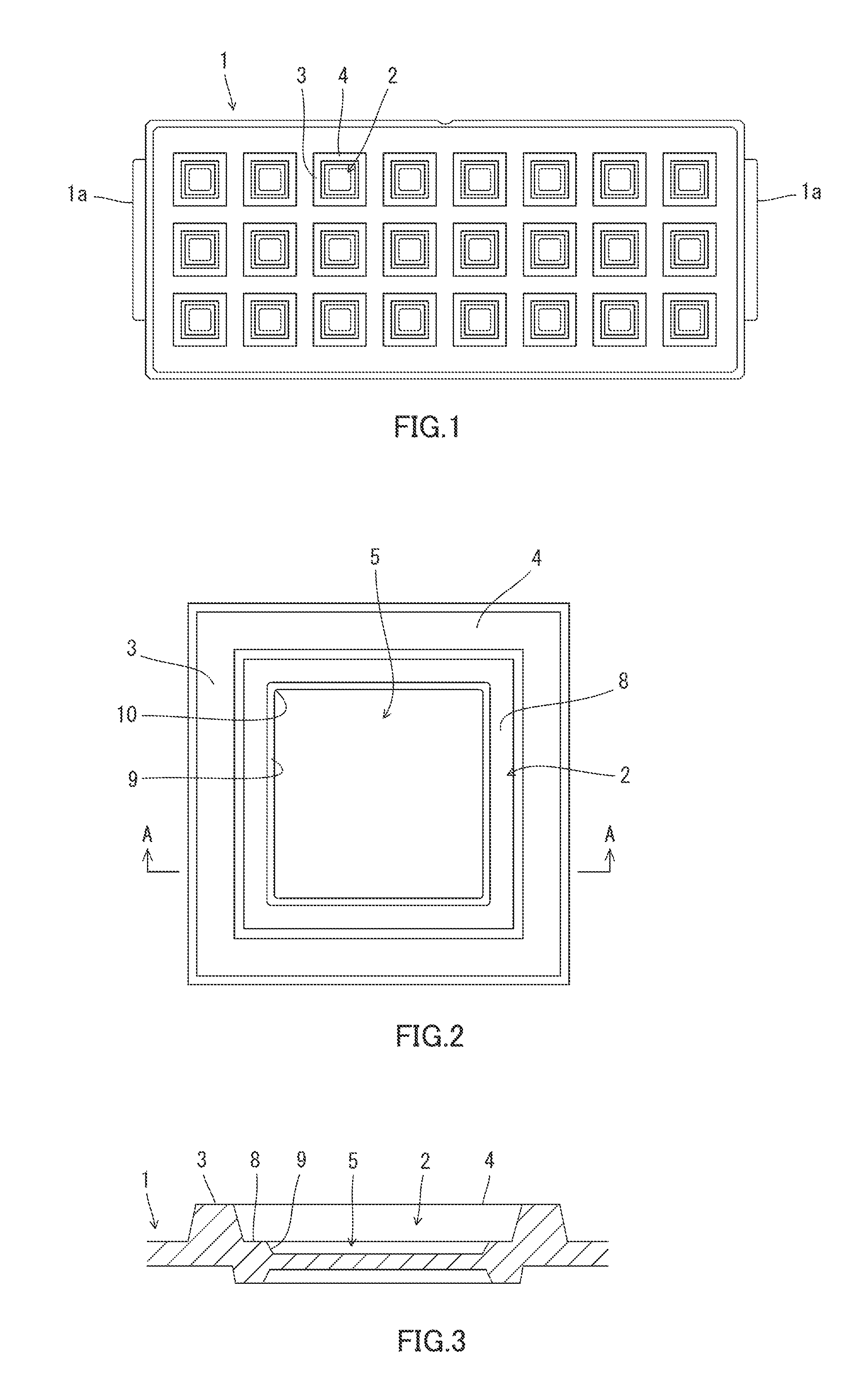
[0031]The tray for semiconductor integrated circuits according to the present invention is used for packaging BGA (Ball Grid Array) semiconductor integrated circuits and thereafter a plurality of trays maybe piled. The upper surface of the tray functions as a packaging container for packaging semiconductor integrated circuits whereas the lower surface thereof functions as a lid of the packaging container.

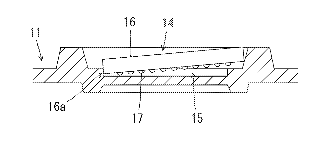
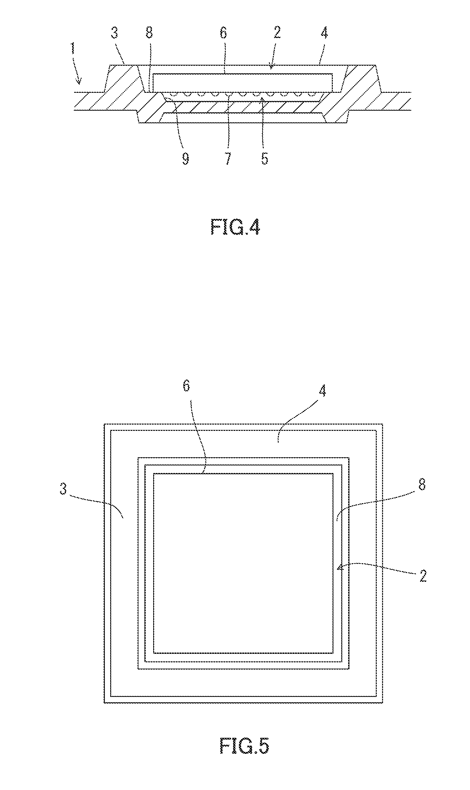
[0032]As illustrated in FIG. 1, the upper surface of a tray 1 is provided with multiple pockets 2 for packaging semiconductor integrated circuits, and the pockets 2 are defined by partition frames 3, 4 with each frame being wider toward the bottom and rising upward so that a semiconductor integrated circuit can fit in the pocket.

[0033]In addition, as illustrated in FIGS. 2 and 3, a pocket ...


PUM


Abstract

The present invention is directed to a tray for semiconductor integrated circuits that enables a BGA semiconductor integrated circuit to be repositioned appropriately in a pocket even if a corner part thereof may fall in a corner part of the recess on the inner bottom surface of a packing pocket. Tapered inner side walls 9 are tilted downward to the inner bottom surface at an angle within the range suggested in FIG. 10 and the ends of adjacent tapered inner side walls 9 are connected by a curving line in the recess 5 provided in a packing pocket 2 of the tray 1 for semiconductor integrated circuits.

Description

BACKGROUND OF THE INVENTION[0001]1. Field of the Invention[0002]The present invention relates to a tray for packaging semiconductor integrated circuits such as ICs, and more specifically, a tray suitable for packaging BGA (Ball Grid Array) semiconductor integrated circuits having multiple terminals on the bottom surface thereof.[0003]2. Description of Related Art[0004]Conventionally, BGA semiconductor integrated circuits are packaged in a tray that is configured as disclosed in Japanese Patent Application Publication No. 11-145315 (Pages 1 to 7, FIGS. 1 to 7) for storage and carriage, for example.[0005]As illustrated in FIG. 11, this tray is adapted to package individual semiconductor integrated circuits in multiple rectangular pockets 14 defined by vertical and horizontal partition frames 12, 13 disposed on the upper surface of the tray 11.[0006]in addition, as illustrated in FIG. 12, on the inner bottom surface of a pocket 14, lies a recess 15 having a flat surface shape which is ...

Claims


Application Information

Patent Timeline
IPC IPC(8): H01L21/673
CPCH01L21/67333
Inventor AZUMA, SEIJI
Owner SHINON CORP
Features
  • R&D
  • Intellectual Property
  • Life Sciences
  • Materials
  • Tech Scout
  • Unparalleled Data Quality
  • Higher Quality Content
  • 60% Fewer Hallucinations
Learn More