Photoelectric conversion substrate, radiation detector, radiographic image capture device, and manufacturing method of radiation detector

a technology of photoelectric conversion substrate and manufacturing method, which is applied in the direction of x/gamma/cosmic radiation measurement, radiographic image capture device, instruments, etc., can solve the problems of high risk of triggering electrostatic destruction, low risk of electrostatic destruction, and electrostatic destruction of photoelectric conversion elements. to achieve the effect of preventing electrostatic destruction of photoelectric conversion elements

Inactive Publication Date: 2013-02-28
FUJIFILM CORP
View PDF11 Cites 15 Cited by
  • Summary
  • Abstract
  • Description
  • Claims
  • Application Information

AI Technical Summary

Benefits of technology

[0026]The present invention can accordingly prevent elec...

Problems solved by technology

However, charge that builds up on the surface of the photoelectric conversion element in a case in which surface treatment is performed on the surface of such a photoelectric conversion substrate may cause electrostatic destruction of the photoelectric conversion element.
For example, the presence of air when plasma processing is performed at atmospheric pressure as surface treatment makes static buildup less likely to occur, and the risk of causing electrostatic destruction is accordingly low.
However, there is a high risk of triggering electrostatic destruction when plasma processing is performed in a vacuum.
Electr...

Method used


Image

  • Photoelectric conversion substrate, radiation detector, radiographic image capture device, and manufacturing method of radiation detector
  • Photoelectric conversion substrate, radiation detector, radiographic image capture device, and manufacturing method of radiation detector
  • Photoelectric conversion substrate, radiation detector, radiographic image capture device, and manufacturing method of radiation detector

Examples


Embodiment Construction

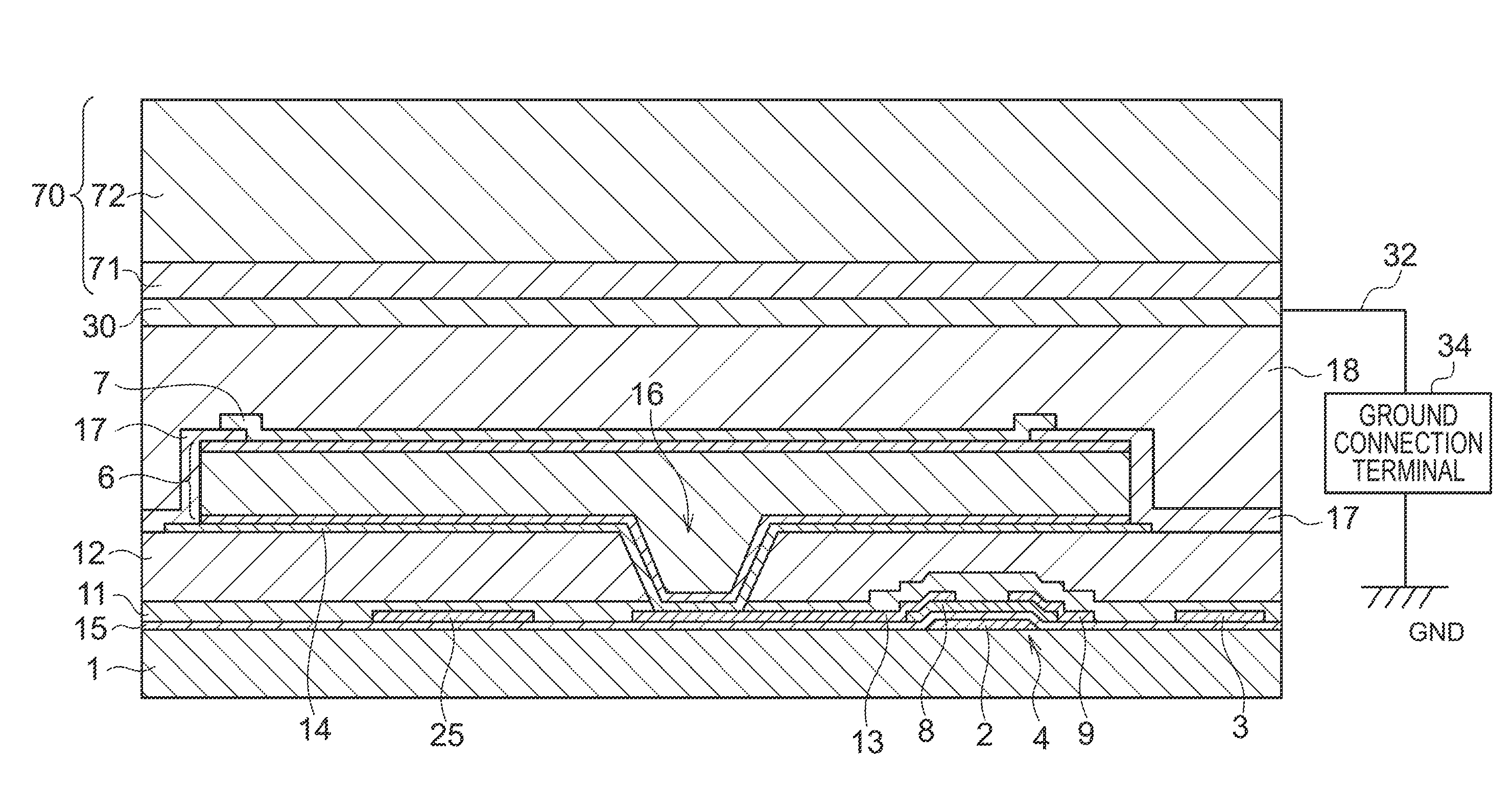
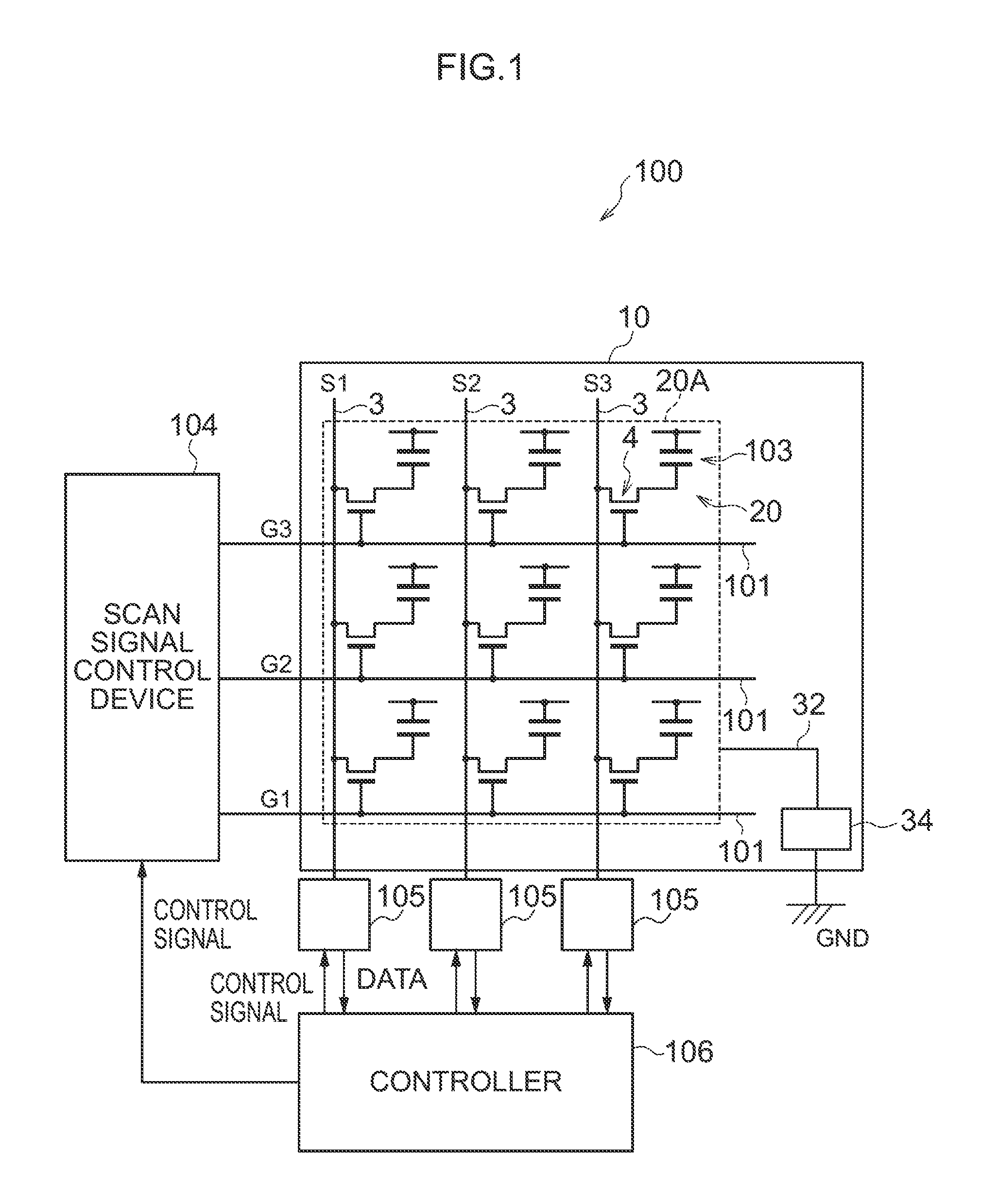
[0044]Outline explanation is given of a radiographic image capture device employing a radiation detector provided with a photoelectric conversion substrate of the present exemplary embodiment. FIG. 1 is a drawing illustrating an example of an overall configuration of a radiographic image capture device employing a radiation detector provided with a photoelectric conversion substrate of the present exemplary embodiment. Note that illustration of a scintillator 70 (described in detail later) has been omitted from in FIG. 1.

[0045]A radiographic image capture device 100 according to the present exemplary embodiment is provided with an indirect-conversion method radiation detector 10, a scan signal control device 104, signal detection circuits 105, and a controller 106. The radiation detector 10 of the present exemplary embodiment is provided with a photoelectric conversion substrate 60 and a scintillator 70.

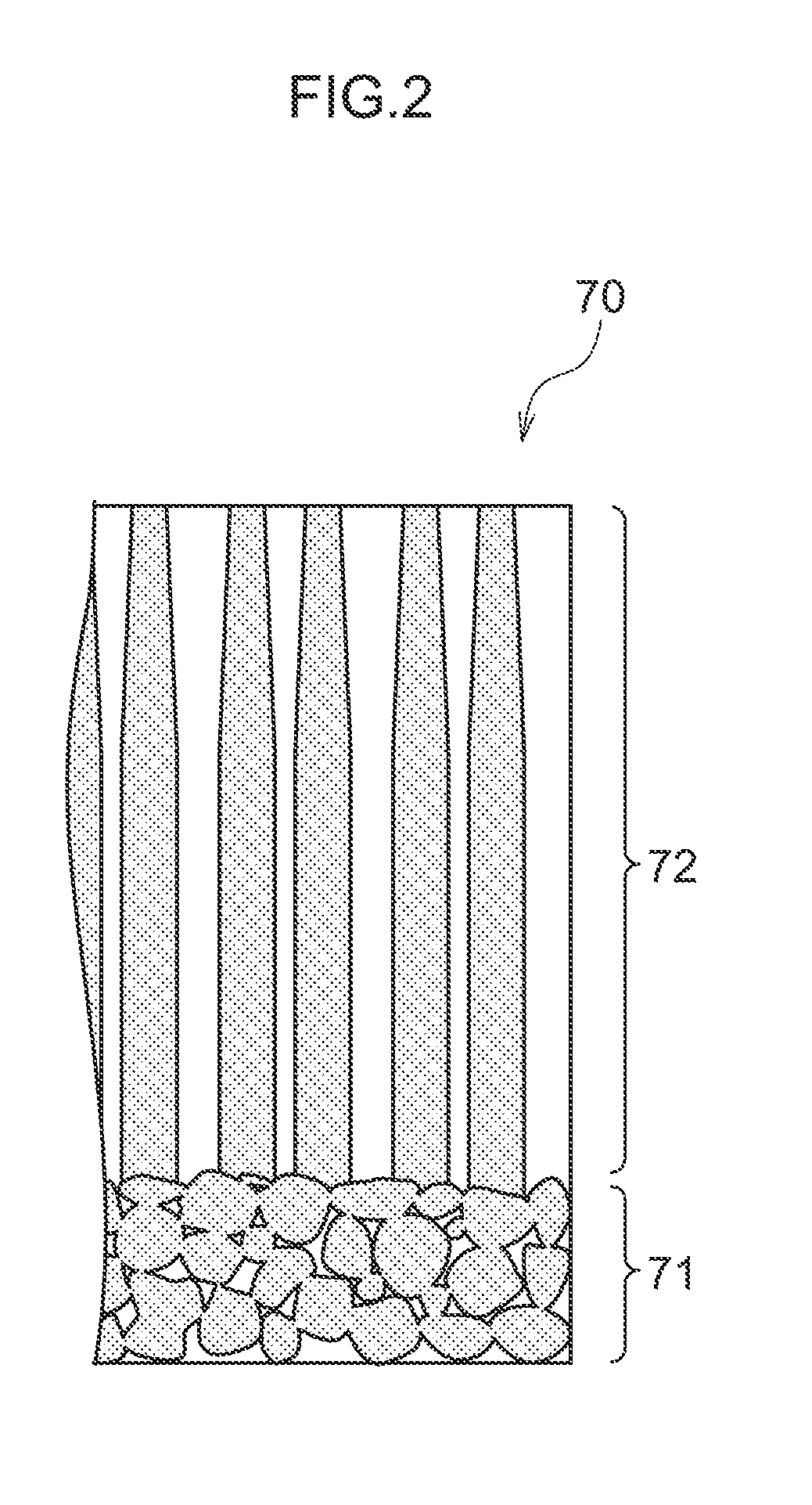
[0046]Explanation is first given regarding the scintillator 70. An example of an...


PUM


Abstract

A photoelectric conversion substrate includes: plural pixels, each provided with a sensor portion and a switching element that are formed on the substrate, the sensor portion including a photoelectric conversion element that generates charge according to illuminated light, and the switching element reading the charge from the sensor portion, a flattening layer that flattens the surface of the substrate having the switching elements and the sensor portions formed thereon, a conducting member formed over the whole face of the flattening layer; and a connection section that connects the conducting member to ground.

Description

CROSS-REFERENCE TO RELATED APPLICATION[0001]This application claims priority under 35 USC 119 from Japanese Patent Application No. 2011-185238 filed on Aug. 26, 2011, the disclosure of which is incorporated by reference herein.BACKGROUND OF THE INVENTION[0002]1. Field of the Invention[0003]The present invention relates to a photoelectric conversion substrate, a radiation detector, a radiographic image capture device and a radiation detector manufacturing method, and in particular relates to a photoelectric conversion substrate, a radiation detector, a radiographic image capture device, and a manufacturing method of a radiation detector employed in such applications as radiographic image capture.[0004]2. Description of the Related Art[0005]Radiographic image capture devices for capturing radiographic images are known in which a radiation detector detects radiation that has been irradiated from a radiation irradiation device and has passed through a subject. As the radiation detector ...

Claims


Application Information

Patent Timeline
IPC IPC(8): G01T1/20G01T1/202H01L31/18H01L27/146
CPCH01L27/308H01L27/14632H01L27/14609G01T1/2018H01L27/14687H10K39/36G01T1/20189
Inventor OHTA, YASUNORISATO, KEIICHIRONISHINO, NAOYUKINAKATSUGAWA, HARUYASU
Owner FUJIFILM CORP
Why Eureka
Try Eureka