Assembly and packaging method and system for optical components

Active Publication Date: 2013-05-02
OTX
View PDF2 Cites 1 Cited by
  • Summary
  • Abstract
  • Description
  • Claims
  • Application Information

AI Technical Summary

Benefits of technology

The present invention provides a method and sub-assembly for aligning an optical fiber with an optical component in a micro-optical sub-assembly. The method involves placing the optical fiber in a groove in the sub-assembly, which is aligned with the optical component. This alignment can be achieved by pressing the fiber firmly into the apex of the groove. The technical effect of this invention is to provide a more accurate and efficient method for aligning optical components and optical fibers in micro-optical sub-assemblies, which can improve the performance and reliability of the optical components.

Problems solved by technology

However as features shrink below 1 μm, diffraction around the mask edges tends to lead to fuzzy lines and ineffective wafer components.
Known techniques for constructing the laser components place the components on the PCB, but have to use expensive specialist machines for very accurate placing.
The tools are expensive.

Method used


Image

  • Assembly and packaging method and system for optical components
  • Assembly and packaging method and system for optical components
  • Assembly and packaging method and system for optical components

Examples


Embodiment Construction

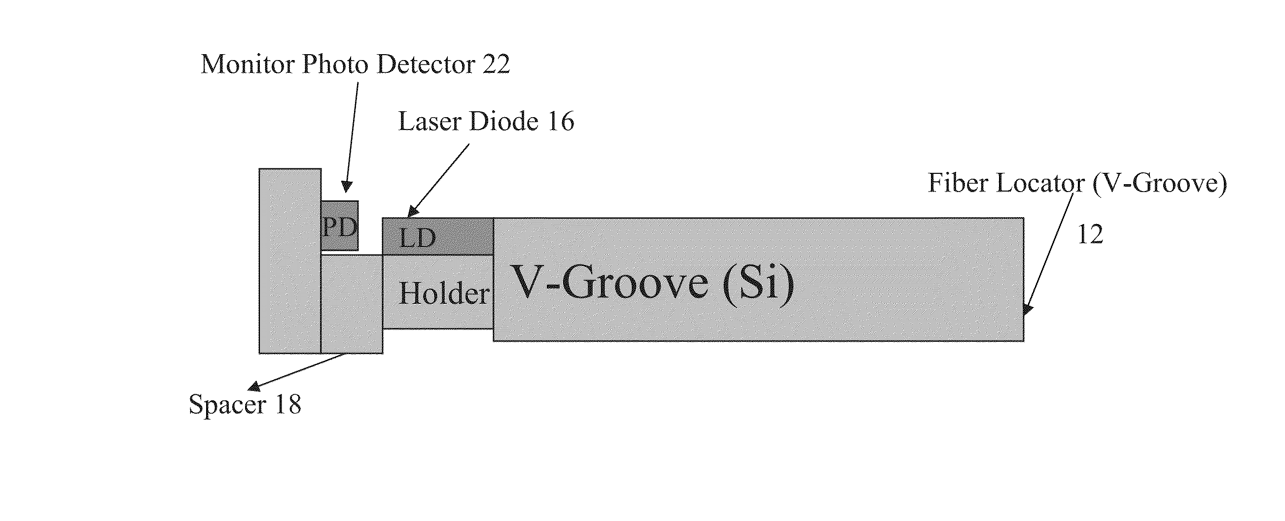
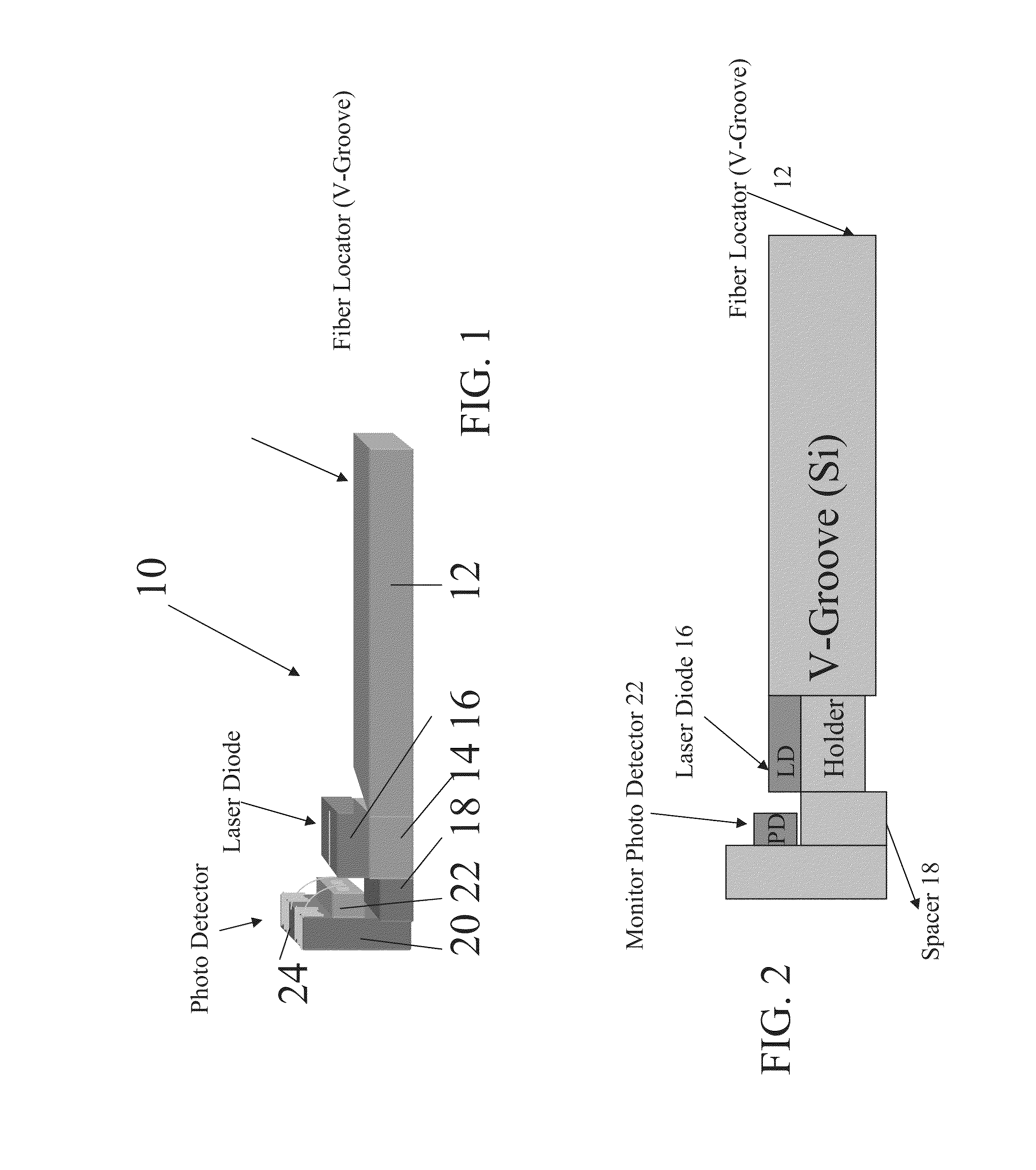
[0059]The present embodiments comprise providing a laser diode, photo-detector or other optical component, aligned with a groove. Then the optical fiber is placed in the groove. The groove may be a v-shaped groove having an apex and the fiber falls into the apex, aligning itself with the optical component.

[0060]The required alignment accuracy is 1 micron. The prior art provides a tool that precisely places the fiber to 1 micron accuracy. The present embodiments may use a placement tool with an accuracy of 50 microns since it merely needs to find the groove and then the groove guides the fiber to the necessary accuracy of 1 micron.

[0061]Although accurate placement of the laser and alignment with the groove are still required, this can be provided using conventional equipment. The obviation of the need for accurate placement of the fiber provides a considerable cost saving in terms of the tools required.

[0062]The principles and operation of an apparatus and method according to the pre...


PUM

PropertyMeasurementUnit
Lengthaaaaaaaaaa
Wavelengthaaaaaaaaaa
Lengthaaaaaaaaaa

Abstract

A method of aligning an optical fiber with an optical component in a micro-optical sub-assembly, comprises: providing a groove in the micro-sub-assembly in alignment with the optical component; and placing the optical fiber in the groove, thereby aligning the optical fiber with the optical component. In this way a placement tool with an accuracy of 50 microns can be used to place an optical fiber with an alignment accuracy of one micron.

Description

FIELD AND BACKGROUND OF THE INVENTION[0001]The present invention relates to an assembly or packaging method and system for optical components and, more particularly, but not exclusively to semiconductor lasers where accurate alignment is required.[0002]The accuracy with which component placing is required in the field of semiconductor lasers depends on the wavelength of the laser concerned. The shorter the wavelength the more accurately the components need to be placed.[0003]Short laser wavelengths are required for a variety of applications. Thus lasers may be used for communications or to draw structures on silicon wafers. For 1.5 μm features, relatively easy to handle laser light of 436 nm is sufficient. However as features shrink below 1 μm, diffraction around the mask edges tends to lead to fuzzy lines and ineffective wafer components. This problem can be solved by using shorter wavelength lasers but then parts have to be more accurately aligned when constructing the laser.[0004...

Claims


Application Information

Patent Timeline
IPC IPC(8): G02B6/36H05K13/04
CPCG02B6/423G02B6/36Y10T29/49002Y10T29/4913H05K13/04
Inventor BENOLIEL, ELI
Owner OTX
Why Eureka
Try Eureka