

Touch sensing panel
- Summary
- Abstract
- Description
- Claims
- Application Information
AI Technical Summary
Benefits of technology
Problems solved by technology
Method used
Image

Examples
Embodiment Construction
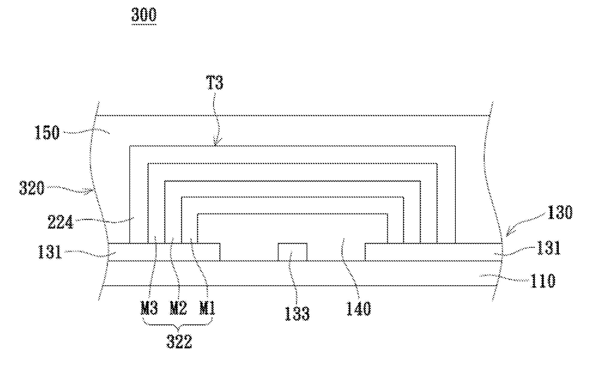
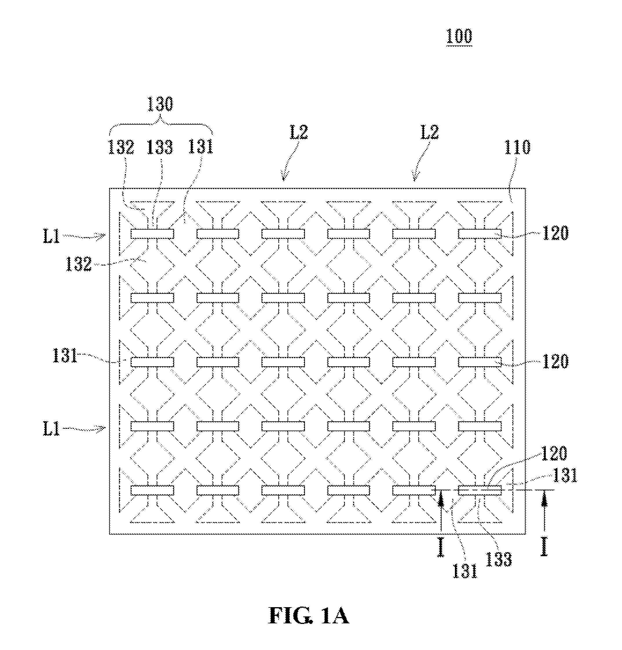
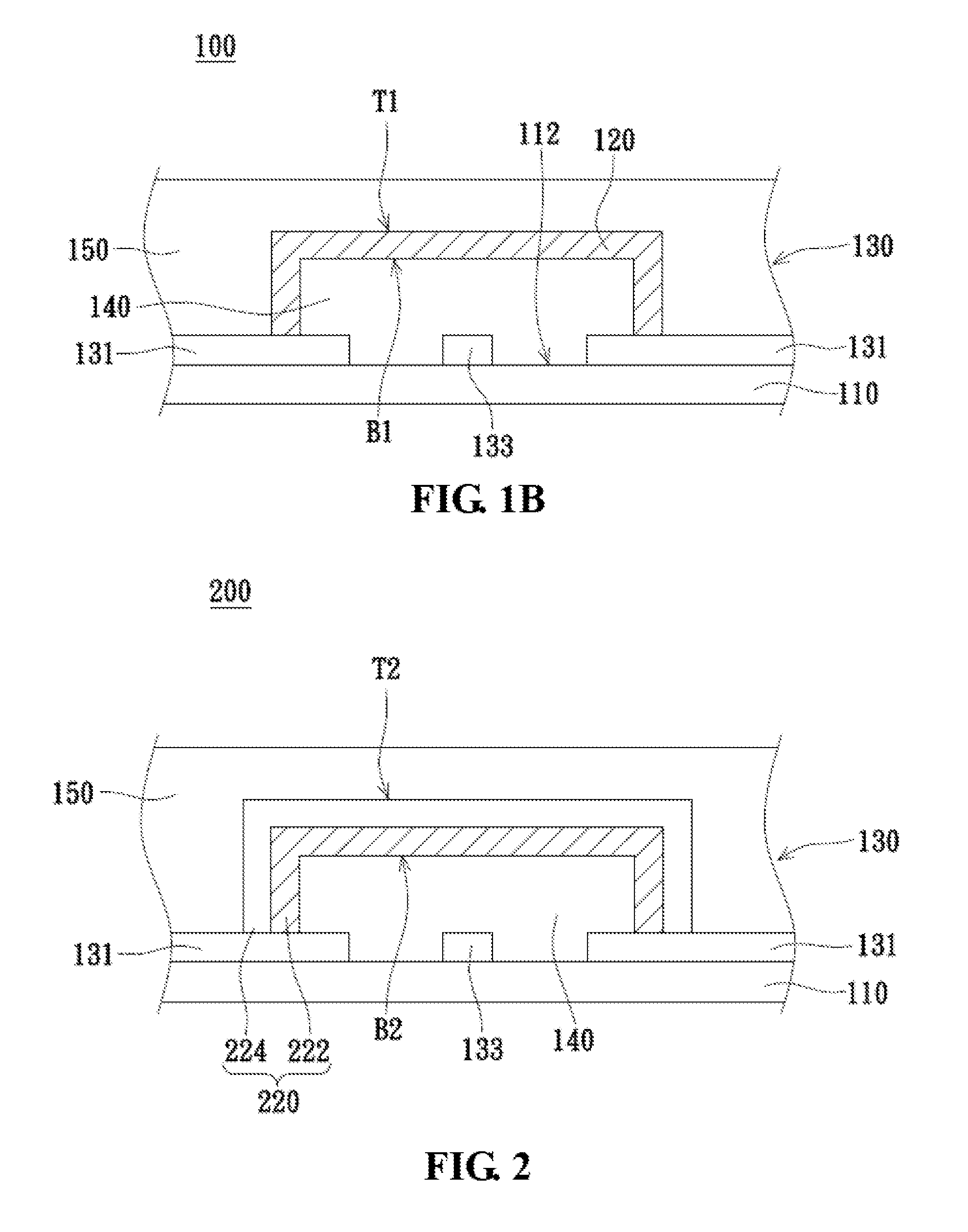
[0015]FIG. 1A is a schematic top view of a touch sensing panel in accordance with a first embodiment of the present disclosure and FIG. 1B is a schematic sectional view of the touch sensing panel sectioned along a line I-I shown in FIG. 1A. Referring to FIG. 1A and FIG. 1B, a touch sensing panel 100 comprises a transparent substrate 110, a plurality of bridging wires 120, and a sensing pattern layer 130. The transparent substrate 110 has a flat surface 112 and the sensing pattern layer 130 is disposed between the bridging wires 120 and the flat surface 112, wherein the transparent substrate 110 is a glass plate or a transparent plastic plate.
[0016]The sensing pattern layer 130 comprises a plurality of first sensing pads 131 arranged along a first axis, a plurality of second sensing pads 132 arranged along a second axis and a plurality of connection parts 133, wherein the first sensing pads 131, the second sensing pads 132, and the connection parts 133 are all disposed on the flat su...
PUM
 Abstract
Description
Claims
Application Information