Organic light emitting diode display device and method for sensing characteristic parameters of pixel driving circuits

a light-emitting diode and display device technology, applied in the direction of instruments, computing, electric digital data processing, etc., can solve the problems of non-uniform luminance between pixels due to process tolerance, non-uniform luminance in the amoled display device, and difficulty in rapidly measuring the amount of current flowing through a number of pixels, so as to correct non-uniform luminance and simple and rapid sensing of characteristic parameters

Active Publication Date: 2013-06-27
LG DISPLAY CO LTD
View PDF5 Cites 201 Cited by
  • Summary
  • Abstract
  • Description
  • Claims
  • Application Information

AI Technical Summary

Benefits of technology

[0011]An object of the present invention is to provide an OLED display device and method for sensing characteristic parameters of pixel driving circuits, which are capable of correcting non-uniformity of luminance through simple and rapid sensing of the characteristic parameters.

Problems solved by technology

In such an AMOLED display device, however, TFT characteristics such as driving TFT threshold voltage Vth and process tolerance factors (e.g., mobility, parasitic capacitance, and channel width / length) are non-uniform among pixels due to process tolerances.
For this reason, non-uniformity of luminance may occur in the AMOLED display device.
For an AMOLED display device having an increased size, however, it is more difficult to rapidly measure amounts of current flowing through a number of pixels.
However, this method has a problem in that there is a difficulty in achieving rapid sensing because the current sensing time is delayed due to parasitic capacitors present in parallel on the power line to achieve increased resolution.
Furthermore, in conventional cases, the system for sensing the characteristics of the driving TFT is complex.
For this reason, after shipment, it is difficult to measure and compensate the characteristics of the driving TFT.

Method used


Image

  • Organic light emitting diode display device and method for sensing characteristic parameters of pixel driving circuits
  • Organic light emitting diode display device and method for sensing characteristic parameters of pixel driving circuits
  • Organic light emitting diode display device and method for sensing characteristic parameters of pixel driving circuits

Examples


first embodiment

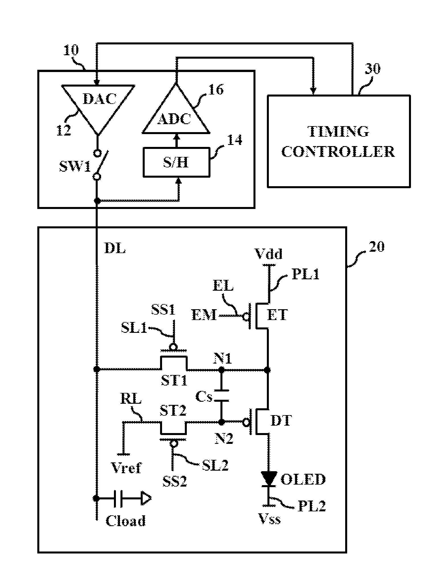
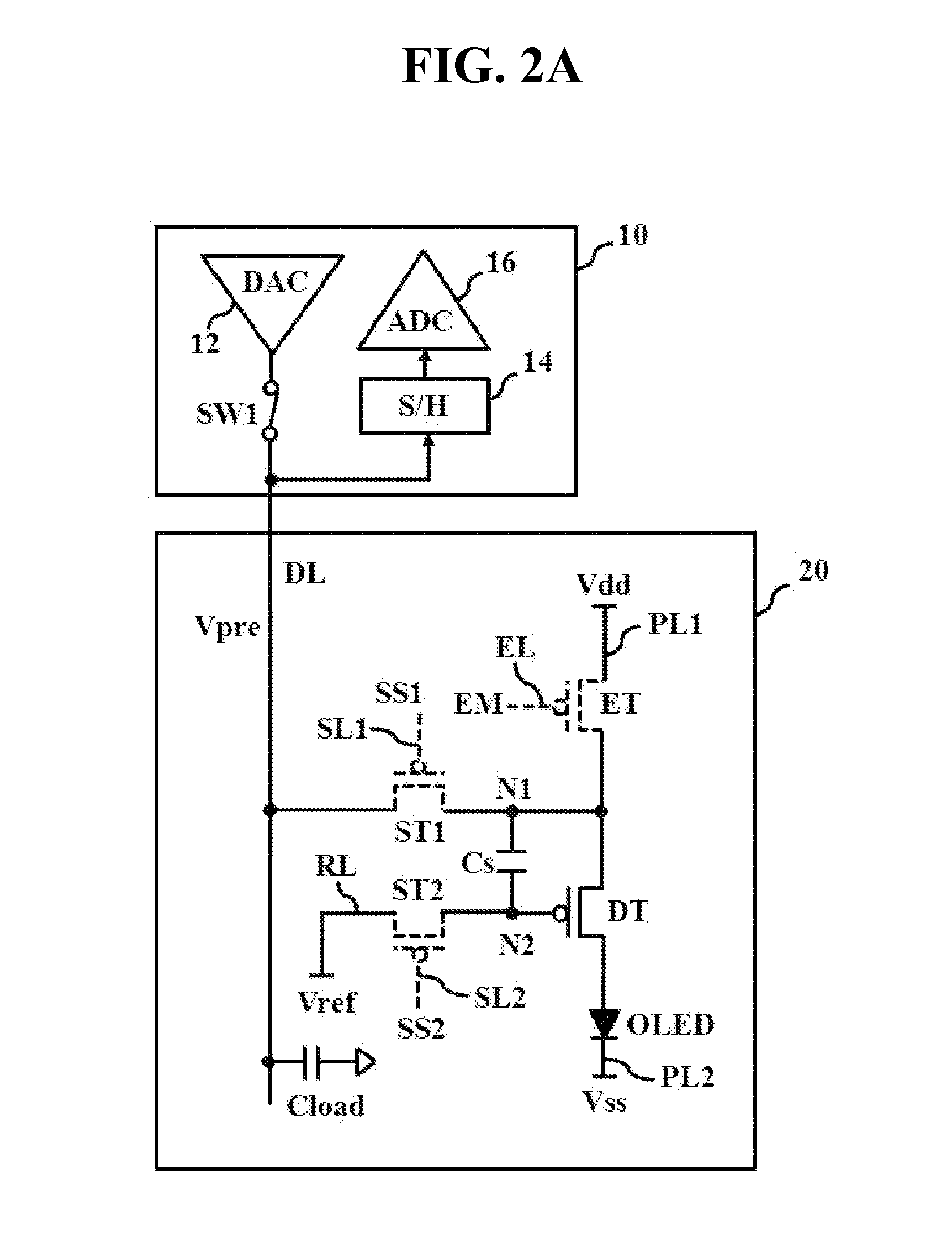
[0061]FIGS. 2A and 2B are circuit diagrams illustrating sequential steps of a method for sensing a threshold voltage Vth of each pixel driving circuit in accordance with the present invention. FIG. 3 is a graph depicting variation in the output voltage on the data line according to passage of time in the case of FIGS. 2A and 2B.

[0062]As shown in FIG. 2A, the DAC 12 supplies the pre-charge voltage Vpre to the data line DL via the turned-on first switch SW1. The pre-charge voltage Vpre may be supplied from an external voltage source to the data line DL via the first switch SW1. Thereafter, as shown in FIG. 2B, the first switch SW is turned off, and the first and second switching TFTs ST1 and ST2 are turned on. Accordingly, the driving TFT DT is driven in a saturated region by the difference voltage between the pre-charge voltage Vpre and the reference voltage Vref, which is charged in the storage capacitor Cs. As a result, the pre-charge voltage Vpre from the data line DL is discharge...

second embodiment

[0064]FIGS. 4A and 4B are circuit diagrams illustrating sequential steps of a method for sensing a threshold voltage Vth of each pixel driving circuit in accordance with the present invention. FIG. 5 is a graph depicting variation in the output voltage on the data line according to passage of time in the case of FIGS. 4A and 4B.

[0065]As shown in FIG. 4A, after supply of the pre-charge voltage Vpre to the data line DL and supply of a first reference voltage Vref1 to the reference voltage line RL, the first and second switching TFTs ST1 and ST2 are turned on. Accordingly, the driving TFT DT is driven. The S / H circuit measures a voltage Vsen1 on the data line DL at a plurality of times when the voltage Vsen1 is saturated in accordance with discharge of the pre-charge voltage Vpre from the data line DL through the first switching TFT ST1, driving TFT DT, and OLED, as shown in FIG. 5(a). The S / H circuit 14 then outputs the measured voltages.

[0066]Thereafter, as shown in FIG. 4B, the pre-...


PUM


Abstract

Disclosed are an OLED display device and method for sensing characteristic parameters of pixel driving circuits. The display device includes a display panel including pixels each having a light emitting element and a pixel driving circuit for independently driving the light emitting element, and a characteristic parameter detecting unit for driving the pixel driving circuit of one of the plural pixels, which is a sensing pixel, sensing a voltage discharged in accordance with characteristics of a driving TFT in the pixel driving circuit of the sensing pixel, on a data line connected to the pixel driving circuit of the sensing pixel, among data lines connected to respective pixel driving circuits of the pixels, and detecting a threshold voltage (Vth) of the driving TFT and a deviation of a process characteristic parameter (k-parameter) of the driving TFT, using the measured voltage.

Description

CROSS-REFERENCE TO RELATED APPLICATIONS[0001]This application claims the benefit of Korean Patent Application No. 10-2011-0142040, filed on Dec. 26, 2011, which is hereby incorporated by reference as if fully set forth herein.BACKGROUND OF THE INVENTION[0002]1. Field of the Invention[0003]The present invention relates to an organic light emitting diode (OLED) display device, and, more particularly, to the OLED display device and a method for sensing characteristic parameters of pixel driving circuits, which are capable of correcting non-uniformity of luminance through simple and rapid sensing of the characteristic parameters.[0004]2. Discussion of the Related Art[0005]An active matrix organic light emitting diode (AMOLED) display device is a self-luminous device in which an organic light emitting layer emits light through re-combination of electrons and holes. Since the AMOLED display device exhibits high luminance, and employs a low driving voltage while having an ultra-slim struct...

Claims


Application Information

Patent Timeline
Patent Type & Authority Applications(United States)
IPC IPC(8): G09G3/32
CPCG09G3/3291G09G2320/0295G09G2300/0861G09G3/3233G09G3/3225G09G3/3258G09G3/3275G09G2320/0233G09G3/30H10K71/00
Inventor YOON, JOONG-SUNKIM, SEUNG-TAEKANG, JI-HYUNLEE, JI-EUN
Owner LG DISPLAY CO LTD
Why Eureka
Try Eureka