Organic light-emitting element, display panel, display device, and manufacturing method for organic light-emitting element

Inactive Publication Date: 2013-07-25
JOLED INC
View PDF3 Cites 4 Cited by
  • Summary
  • Abstract
  • Description
  • Claims
  • Application Information

AI Technical Summary

Benefits of technology

The patent describes a method for manufacturing an organic light-emitting element with a long useful life. The method involves using a planarization film made of an inorganic material, which prevents the planarization film from shifting and maintains its planarity during the process. This results in a highly planarized upper surface of the organic light-emitting element, ultimately improving its light-emitting properties. Additionally, the use of an inorganic material prevents the planarization film from absorbing water, reducing its expansion, contraction, and bubble formation during the process.

Problems solved by technology

However, the display device pertaining to conventional technology and having the planarization film 903, which is an organic film, is prone to expansion, contraction, and bubble formation due to peeling and to absorption of water produced during the planarization film 903 formation process.
This causes a decrease in useful life.
However, although such technology of covering the upper surface of the planarization film with a protective film may interrupt the passage of water between the planarization film and the organic EL layer, the planarization film made of organic material is made unable to retreat from any water absorbed into the device.
This does not resolve the problem of contraction and expansion due to heat, and does not preserve the planarity of the upper surface.
However, as shown, when the planarization film 913 is made of an inorganic material, the upper surface with respect to the Z dimension 913f conforms to the irregularities of the TFT layer 901, and is thus unable to preserve planarity.

Method used


Image

  • Organic light-emitting element, display panel, display device, and manufacturing method for organic light-emitting element
  • Organic light-emitting element, display panel, display device, and manufacturing method for organic light-emitting element
  • Organic light-emitting element, display panel, display device, and manufacturing method for organic light-emitting element

Examples


embodiment

[0083]The following describes an Embodiment of the present disclosure by means of example.

[0084]The following Embodiment is used solely as an example selected for ease of comprehension with respect to the configuration, usage, and effects of the present disclosure. No particular limitation is intended.

1. Overview of Display Device 1

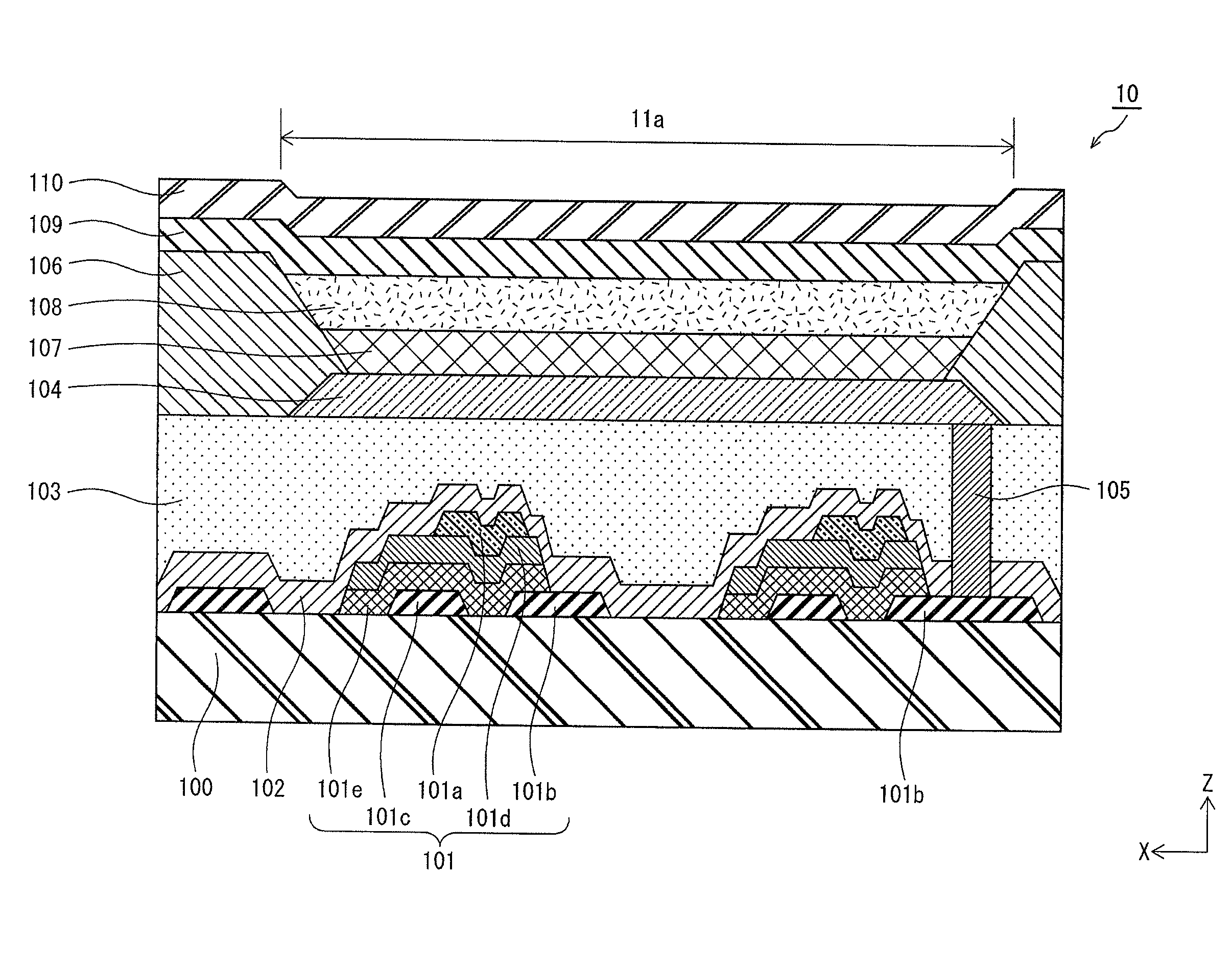
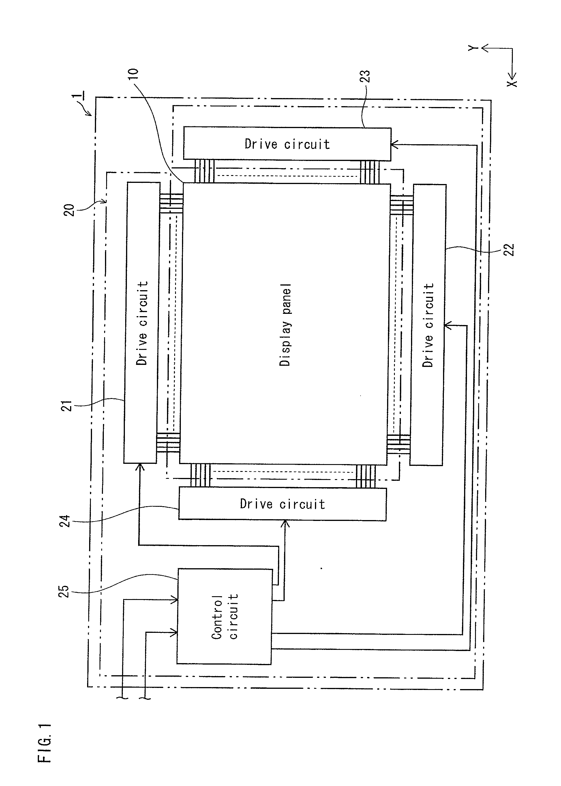
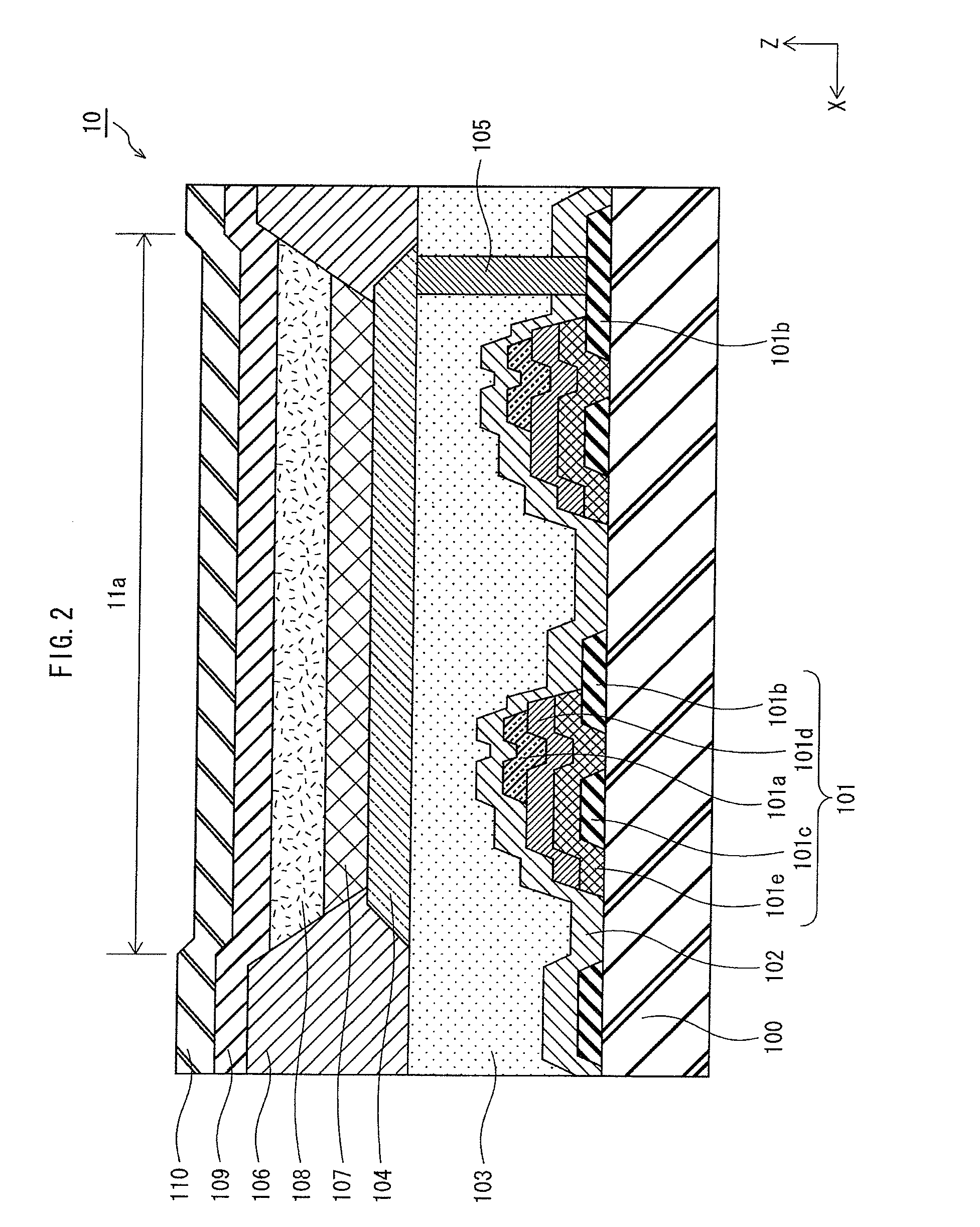
[0085]The following describes a display device 1 pertaining to the Embodiment with reference to FIG. 1.

[0086]As shown, the display device 1 includes a display panel 10 and a drive control unit 20 connected thereto. The display panel 10 is an organic electroluminescence panel (hereinafter, EL panel) employing the phenomenon of organic material electroluminescence, in which a plurality of organic EL elements are arranged.

[0087]The drive control unit 20 includes four drive circuits 21-24 and a control circuit 25.

[0088]In practice, no limitation is intended regarding the arrangement and connection relationship of the drive control unit 20 to the display panel...


PUM


Abstract

A planarization film is formed as a silicon oxide monolayer using, for instance, a spin coat method, through, for example, applying a silicon-containing organic solvent to an upper portion of a TFT layer and planarizing an upper surface of a resist film made up of a silicon-containing organic solvent, heating a predetermined processing fluid, e.g., peroxymonosulfuric acid, and discharging the processing fluid heated to, for example, 150° C., onto the planarized upper surface of the resist film such that organic components of the resist film are dissolved while silicon in the resist film is oxidized by the processing fluid.

Description

CROSS REFERENCE TO RELATED APPLICATION[0001]This is a continuation application of PCT Application No. PCT / JP2010 / 004279 filed Jun. 29, 2010, designating the United States of America, the disclosure of which, including the specification, drawings and claims, is incorporated herein by reference in its entirety.TECHNICAL FIELD[0002]The present disclosure relates to an organic light-emitting element, a display panel, a display device, and a manufacturing method for an organic light-emitting element.DESCRIPTION OF THE RELATED ART[0003]In recent years, progress and discoveries have been made in the field of display devices that employ the phenomenon of organic material electroluminescence. In such a display device, each sub-pixel includes an anode and a cathode having an organic electroluminescence element (hereinafter, organic EL element) that includes an organic light-emitting layer sandwiched therebetween. The operation of such a display device that includes an organic EL layer involve...

Claims


Application Information

Patent Timeline
IPC IPC(8): H01L51/52H01L51/56
CPCH01L27/3258H01L51/5253H01L27/1292H01L27/1248H01L51/56H10K59/124H10K71/00H10K59/873H10K50/844
Inventor SUGANO, KOU
Owner JOLED INC
Why Eureka
Try Eureka