Wiring board and method for manufacturing wiring board

Active Publication Date: 2013-08-01
IBIDEN CO LTD
View PDF6 Cites 8 Cited by
  • Summary
  • Abstract
  • Description
  • Claims
  • Application Information

AI Technical Summary

Benefits of technology

This patent relates to a type of wiring board that has conductive patterns and a layer of solder-resist. The solder-resist layer has an edge that borders an opening and has a concave-convex shape. The effects of this design include improved soldering, reduced bridging, and better protection of the conductive patterns. The manufacturing process involves forming the conductive patterns on an insulation layer and then adding the solder-resist layer with the opening to expose the conductive patterns.

Problems solved by technology

In small-size electronic devices typified by mobile communication terminals, mounting space is limited for components that form electronic circuits.

Method used


Image

  • Wiring board and method for manufacturing wiring board
  • Wiring board and method for manufacturing wiring board
  • Wiring board and method for manufacturing wiring board

Examples


Embodiment Construction

[0044]The embodiments will now be described with reference to the accompanying drawings, wherein like reference numerals designate corresponding or identical elements throughout the various drawings.

[0045]For description purposes, a coordinate system is used where axes (X, Y, Z) intersect at right angles with each other.

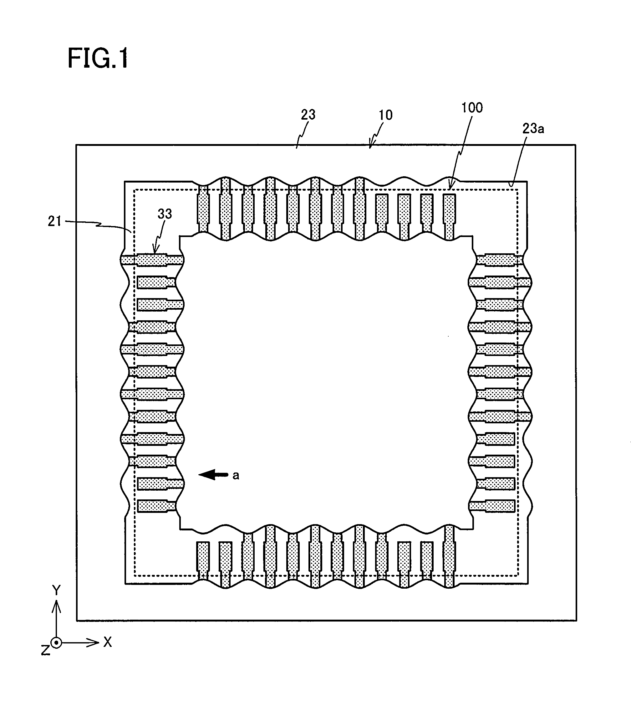
[0046]FIG. 1 shows a plan view of wiring board 10 according to the present embodiment. Wiring board 10 is a printed wiring board. On an upper surface of wiring board 10 (a surface on the (+Z) side), electronic component 100 is flip-chip mounted.

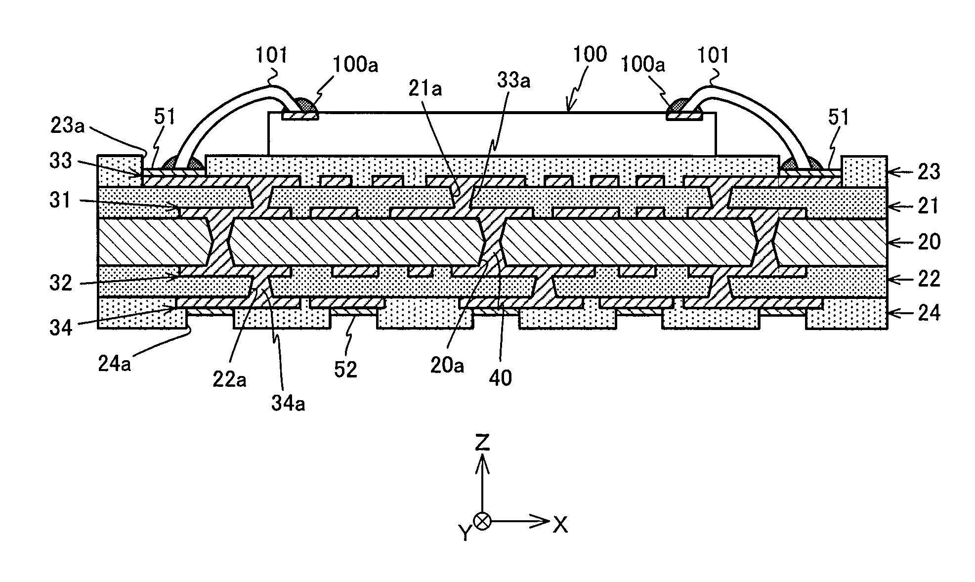
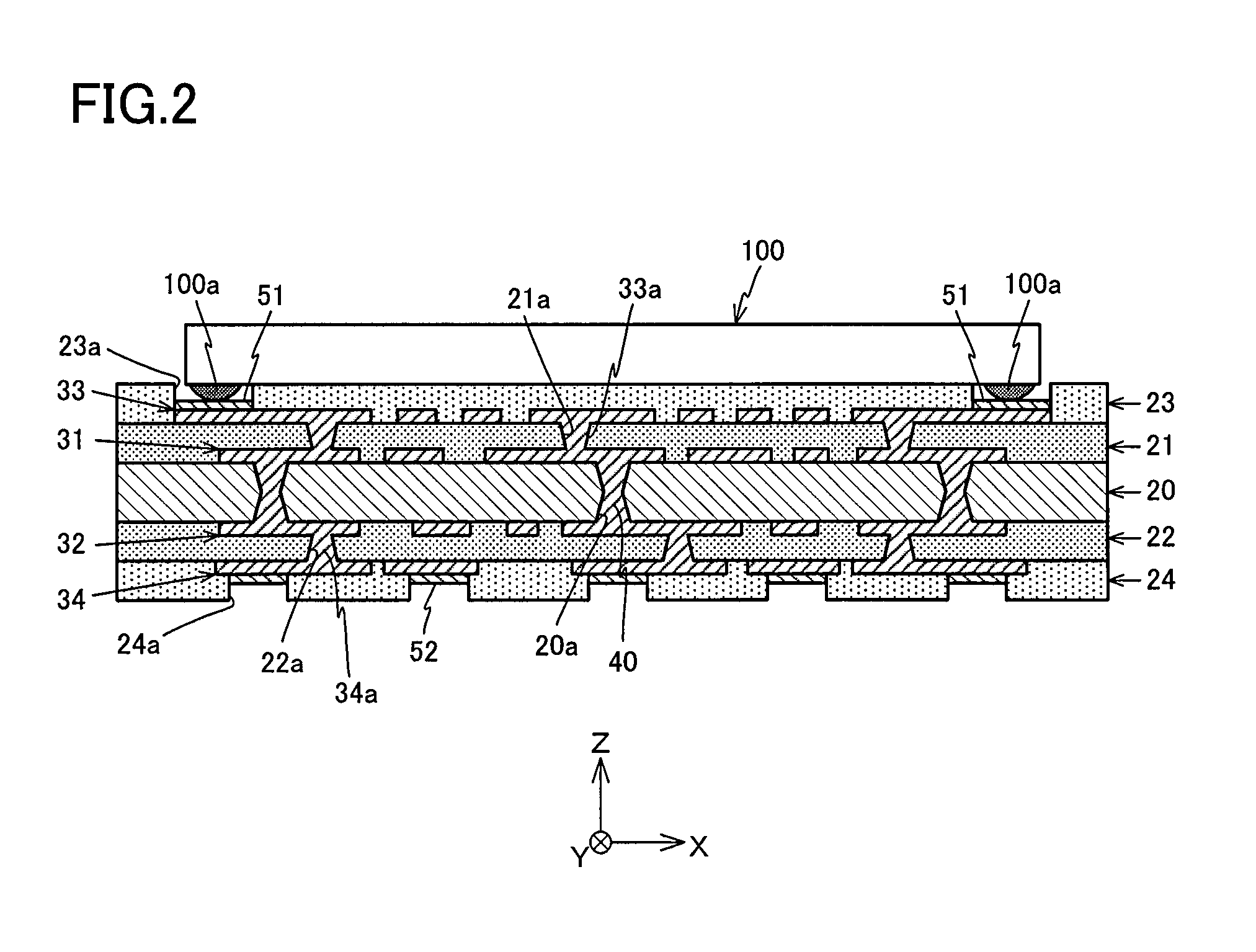
[0047]FIG. 2 is a ZX cross-sectional view of wiring board 10. As shown in FIG. 2, wiring board 10 has core substrate 20, conductive patterns (31, 32, 33, 34), insulation layers (21, 22) and solder-resist layers (23, 24).

[0048]Core substrate 20 is formed by impregnating glass fiber or aramid fiber, for example, with epoxy resin. As shown in FIG. 2, penetrating hole (20a) is formed in core substrate 20.

[0049]Through-hole conduct...


PUM

PropertyMeasurementUnit
Shapeaaaaaaaaaa
Electrical conductoraaaaaaaaaa
Areaaaaaaaaaaa

Abstract

A wiring board includes an interlayer insulation layer, conductive patterns formed on the interlayer insulation layer, and a solder-resist layer formed on the interlayer insulation layer and having an opening partially exposing the conductive patterns. The solder-resist layer has an edge portion bordering the opening and intersecting the conductive patterns, and the edge portion of the solder-resist layer has a concavo-convex shape having convex portions and concave portions such that the convex portions and the concave portions are alternately intersecting the conductive patterns.

Description

CROSS-REFERENCE TO RELATED APPLICATIONS[0001]The present application is based on and claims the benefit of priority to U.S. Application No. 61 / 552,841, filed Oct. 28, 2011, the entire contents of which are incorporated herein by reference.BACKGROUND OF THE INVENTION[0002]1. Field of the Invention[0003]The present invention relates to a wiring board and its manufacturing method.[0004]2. Discussion of the Background[0005]In small-size electronic devices typified by mobile communication terminals, mounting space is limited for components that form electronic circuits. Japanese Laid-Open Patent Publication No. 2000-77471 describes a wiring board where a wider pad is formed in the center of a conductor exposed through an opening of a solder-resist layer. The contents of Japanese Laid-Open Patent Publication No. 2000-77471 are incorporated herein by reference in their entirety in this application.SUMMARY OF THE INVENTION[0006]According to one aspect of the present invention, a wiring boar...

Claims


Application Information

Patent Timeline
IPC IPC(8): H05K1/02H05K3/10
CPCH05K1/114H05K3/3452H05K3/4652H05K1/0296Y10T29/49155H01L2224/48091H05K3/10H01L2924/00014H01L23/12H05K1/18H05K3/46
Inventor FURUTA, TORUTAKAGI, FUMITAKA
Owner IBIDEN CO LTD
Why Eureka
Try Eureka