AI technical title is built by Patsnap AI team. It summarizes the technical point description of the patent document.
a technology of electro-optic displays and displays, applied in the direction of electric digital data processing, instruments, computing, etc., can solve the problems of preventing their widespread use, inadequate service life of these displays, gas-based electrophoretic media being susceptible to the same types of problems, etc., to reduce or eliminate edge artifacts, reduce the visibility of edge artifacts, and fast display switching
Active Publication Date: 2013-08-01
E INK CORPORATION
View PDF6 Cites 175 Cited by
Summary
Abstract
Description
Claims
Application Information
AI Technical Summary
This helps you quickly interpret patents by identifying the three key elements:
Problems solved by technology
Method used
Benefits of technology
Benefits of technology
The patent text describes different methods for reducing or eliminating edge artifacts in bistable electro-optic displays. These methods include using balanced pulse pairs, applying extra pixels along a straight edge, and allowing pixels to deviation temporarily from DC balance. These methods can improve the quality and responsiveness of the display, making it easier to produce high-quality visuals.
Problems solved by technology
Nevertheless, problems with the long-term image quality of these displays have prevented their widespread usage.
For example, particles that make up electrophoretic displays tend to settle, resulting in inadequate service-life for these displays.
Such gas-based electrophoretic media appear to be susceptible to the same types of problems due to particle settling as liquid-based electrophoretic media, when the media are used in an orientation which permits such settling, for example in a sign where the medium is disposed in a vertical plane.
Indeed, particle settling appears to be a more serious problem in gas-based electrophoretic media than in liquid-based ones, since the lower viscosity of gaseous suspending fluids as compared with liquid ones allows more rapid settling of the electrophoretic particles.
However, inevitably there is some error in writing images on an impulse-driven display.
(a) Prior State Dependence;With at least some electro-optic media, the impulse required to switch a pixel to a new optical state depends not only on the current and desired optical state, but also on the previous optical states of the pixel.
(b) Dwell Time Dependence;With at least some electro-optic media, the impulse required to switch a pixel to a new optical state depends on the time that the pixel has spent in its various optical states. The precise nature of this dependence is not well understood, but in general, more impulse is required the longer the pixel has been in its current optical state.
(c) Temperature Dependence;The impulse required to switch a pixel to a new optical state depends heavily on temperature.
(d) Humidity Dependence;The impulse required to switch a pixel to a new optical state depends, with at least some types of electro-optic media, on the ambient humidity.
(e) Mechanical Uniformity;The impulse required to switch a pixel to a new optical state may be affected by mechanical variations in the display, for example variations in the thickness of an electro-optic medium or an associated lamination adhesive. Other types of mechanical non-uniformity may arise from inevitable variations between different manufacturing batches of medium, manufacturing tolerances and materials variations.
(f) Voltage Errors;The actual impulse applied to a pixel will inevitably differ slightly from that theoretically applied because of unavoidable slight errors in the voltages delivered by drivers.
General grayscaleimage flow suffers from an “accumulation of errors” phenomenon.
This accumulation of errors phenomenon applies not only to errors due to temperature, but also to errors of all the types listed above.
As described in the aforementioned U.S. Pat. No. 7,012,600, compensating for such errors is possible, but only to a limited degree of precision.
For example, temperature errors can be compensated by using a temperature sensor and a lookup table, but the temperature sensor has a limited resolution and may read a temperature slightly different from that of the electro-optic medium.
Similarly, prior state dependence can be compensated by storing the prior states and using a multi-dimensional transition matrix, but controller memory limits the number of states that can be recorded and the size of the transition matrix that can be stored, placing a limit on the precision of this type of compensation.
However, certain problems remain in this type of GL drive scheme.
Firstly, as discussed in detail in some of the aforementioned MEDEOD applications, bistable electro-optic media are typically not completely bistable, and pixels placed in one extreme optical state gradually drift, over a period of minutes to hours, towards an intermediate gray level.
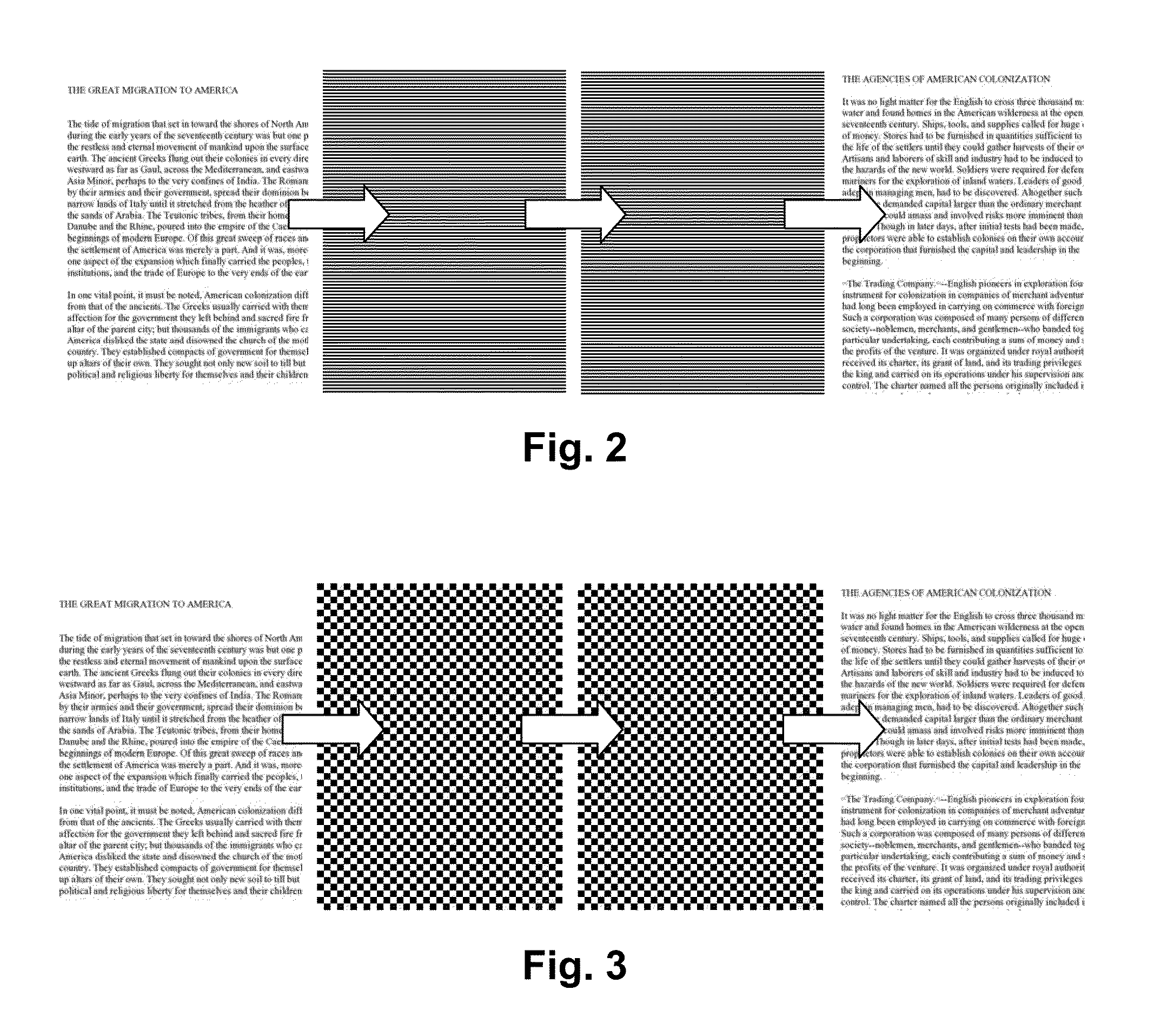
Secondly, when an undriven pixel lies adjacent a pixel which is being updated, a phenomenon known as “blooming” occurs, in which the driving of the driven pixel causes a change in optical state over an area slightly larger than that of the driven pixel, and this area intrudes into the area of adjacent pixels.
Over time, such edge effects become visually distracting and must be cleared.
Unfortunately, use of such an occasional GC update reintroduces the problem of a “flashy” update, and indeed the flashiness of the update may be heightened by the fact that the flashy update only occurs at long intervals.
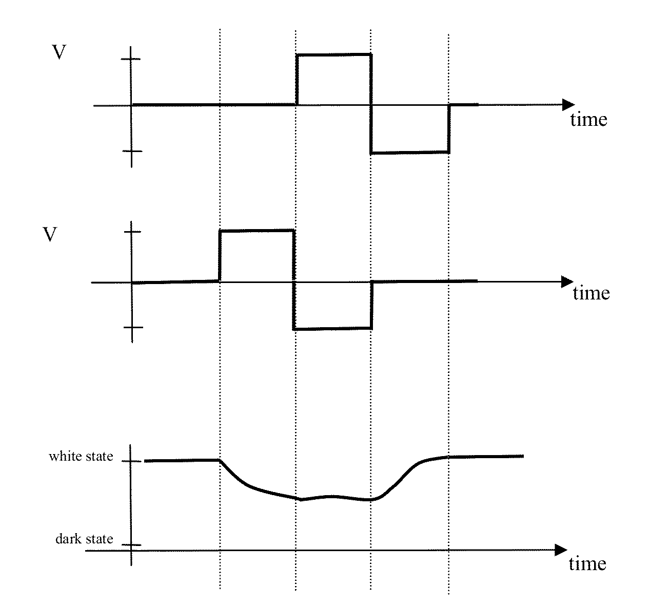
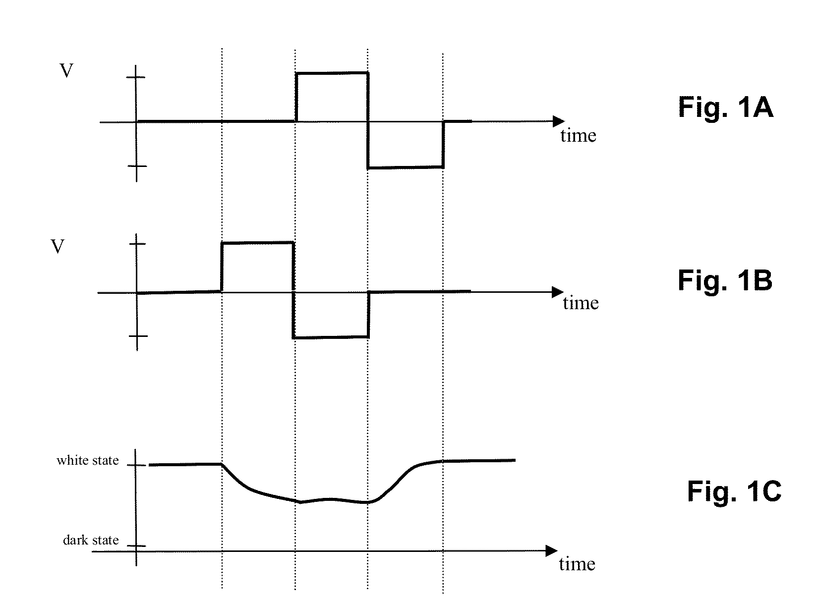
However, there is an additional complication in attempting to solve the aforementioned problems, namely the need for overall DC balance.
As discussed in many of the aforementioned MEDEOD applications, the electro-optic properties and the working lifetime of displays may be adversely affected if the drive schemes used are not substantially DC balanced (i.e., if the algebraic sum of the impulses applied to a pixel during any series of transitions beginning and ending at the same gray level is not close to zero).
Method used
Image
Click on the blue label to locate the original text in one second.
Reading with bidirectional positioning of images and text.
Examples
Embodiment Construction
[0074]It will be apparent from the foregoing that the present invention provides a plurality of discrete inventions relating to driving electro-optic displays and apparatus for use in such methods. These various inventions will be described separately below, but it will be appreciated that a single display may incorporate more than one of these inventions. For example, it will readily be apparent that a single display could make use of the selective general update and straight edge extra pixels drive scheme methods of the present invention and use the arbitrary region assignment controller of the invention.
[0075]Part A: Selective General Update Method of the Invention
[0076]As explained above, the selective general update (SGU) method of the invention is intended for use in an electro-optic display having a plurality of pixels. The method makes use of a first drive scheme, in which all pixels are driven at each transition, and a second drive scheme, in which pixels undergoing some tr...
PUM
Abstract
A variety of methods for driving electro-optic displays so as to reduce visible artifacts are described. Such methods include (a) applying a first drive scheme to a non-zero minor proportion of the pixels of the display and a second drive scheme to the remaining pixels, the pixels using the first drive scheme being changed at each transition; (b) using two different drive schemes on different groups of pixels so that pixels in differing groups undergoing the same transition will not experience the same waveform; (c) applying either a balanced pulse pair or a top-off pulse to a pixel undergoing a white-to-white transition and lying adjacent a pixel undergoing a visible transition; (d) driving extra pixels where the boundary between a driven and undriven area would otherwise fall along a straight line; and (e) driving a display with both DC balanced and DC imbalanced drive schemes, maintaining an impulse bank value for the DC imbalance and modifying transitions to reduce the impulse bank value.
Application Information
Patent Timeline
Application Date:The date an application was filed.
Publication Date:The date a patent or application was officially published.
First Publication Date:The earliest publication date of a patent with the same application number.
Issue Date:Publication date of the patent grant document.
PCT Entry Date:The Entry date of PCT National Phase.
Estimated Expiry Date:The statutory expiry date of a patent right according to the Patent Law, and it is the longest term of protection that the patent right can achieve without the termination of the patent right due to other reasons(Term extension factor has been taken into account ).
Invalid Date:Actual expiry date is based on effective date or publication date of legal transaction data of invalid patent.
Patent Type & AuthorityApplications(United States)

