Method of Inspecting Chip Defects
a chip and defect technology, applied in the field of chip defects inspection, can solve the problems of poor performance of defect inspection and prior arts that do not meet users' actual use requirements, and achieve the effect of improving performance and accuracy of inspections
- Summary
- Abstract
- Description
- Claims
- Application Information
AI Technical Summary
Benefits of technology
Problems solved by technology
Method used
Image

Examples
Embodiment Construction
[0017]The following descriptions of the preferred embodiment are provided to understand the features and the structures of the present invention.
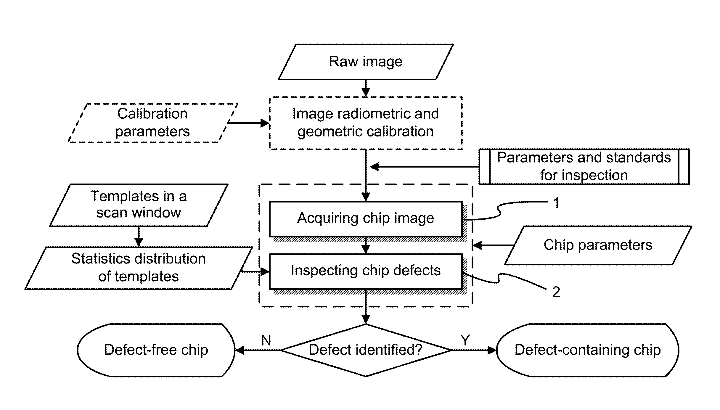
[0018]Please refer to FIG. 1, which is a flow view showing a preferred embodiment according to the present invention. As shown in the figure, the present invention is a method of inspecting chip defects, where chip defects are inspected based on a binary chip edge image to greatly improve inspection performance and inspection accuracy. On using the present invention, based on a raw image of a chip and a raw edge image of the chip, defects on the chip exceeding inspection criteria are inspected quantitatively and precisely through the following steps:
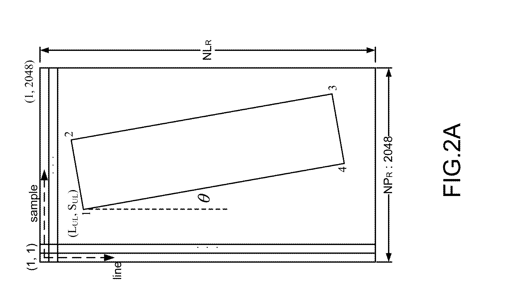
[0019](a) Acquiring images of chip 1: An edge image of a chip is acquired through edge detection; chip boundaries derivation; chip corners derivation; parameters derivation of affine transformation; and chip image segmentation. Therein, a raw image of the chip is processed through the edge detec...
PUM
 Abstract
Description
Claims
Application Information