Methods and Apparatus of Wafer Level Package for Heterogeneous Integration Technology

a technology of heterogeneous integration and wafer level, applied in electrical devices, semiconductor devices, semiconductor/solid-state device details, etc., can solve problems such as inability to provide a larger heigh

Active Publication Date: 2013-10-10
TAIWAN SEMICON MFG CO LTD
View PDF8 Cites 148 Cited by
  • Summary
  • Abstract
  • Description
  • Claims
  • Application Information

AI Technical Summary

Problems solved by technology

Such techniques may require a larger height wh

Method used


Image

  • Methods and Apparatus of Wafer Level Package for Heterogeneous Integration Technology
  • Methods and Apparatus of Wafer Level Package for Heterogeneous Integration Technology
  • Methods and Apparatus of Wafer Level Package for Heterogeneous Integration Technology

Examples


Embodiment Construction

[0009]The making and using of the embodiments of the present disclosure are discussed in detail below. It should be appreciated, however, that the embodiments of the present disclosure provide many applicable concepts that can be embodied in a wide variety of specific contexts. The specific embodiments discussed are merely illustrative of specific ways to make and use the disclosure, and do not limit the scope of the disclosure.

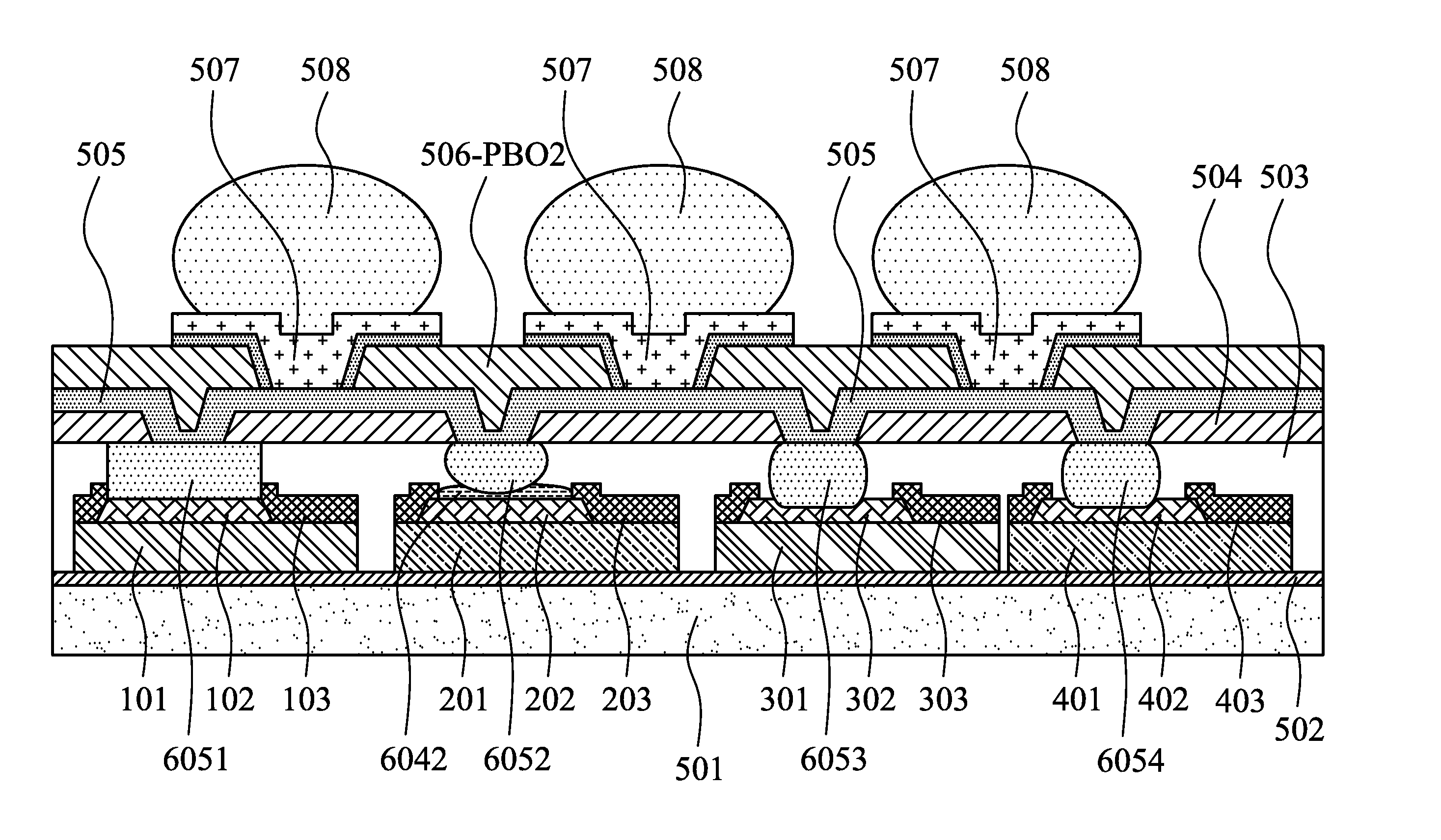
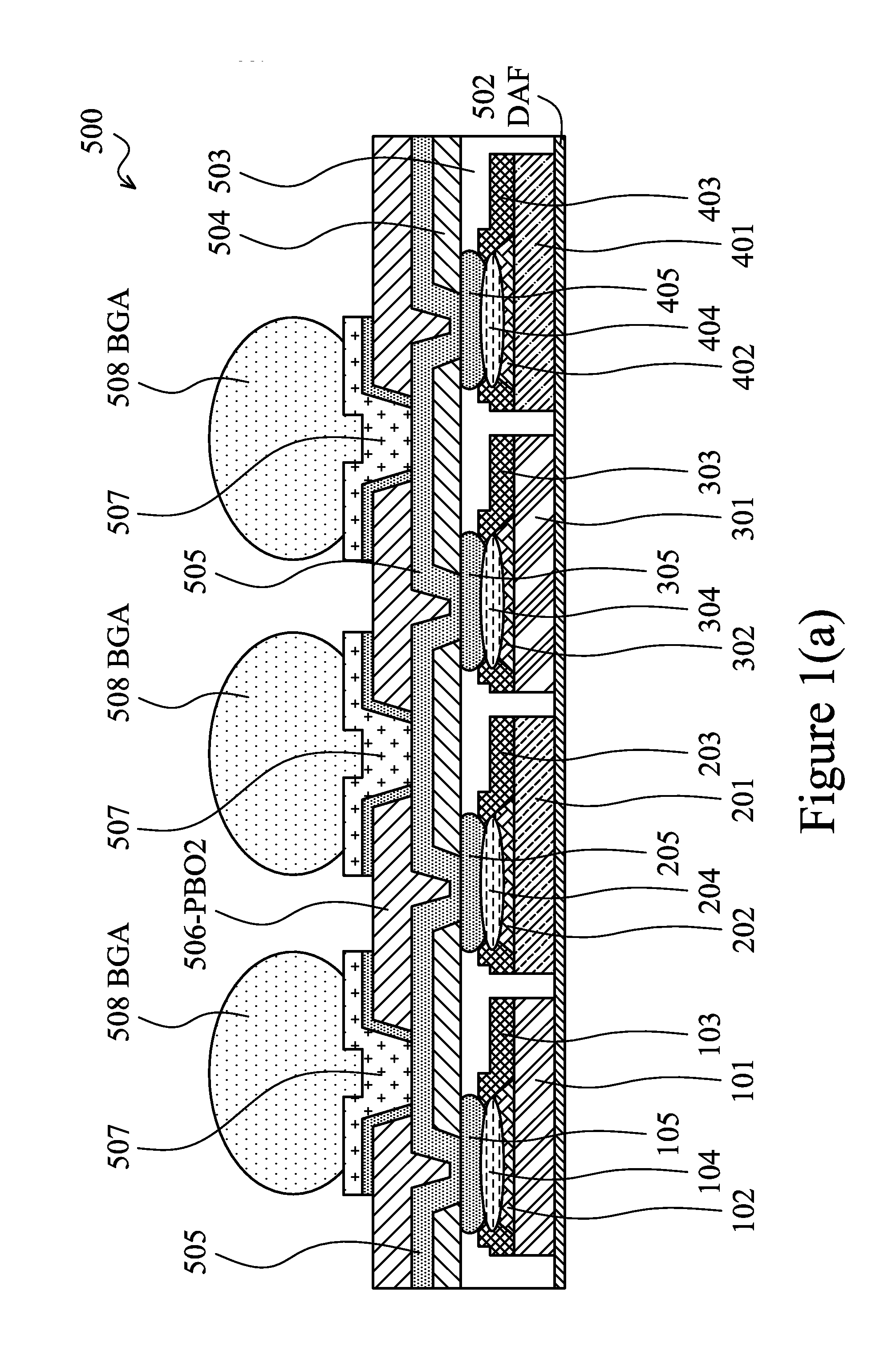
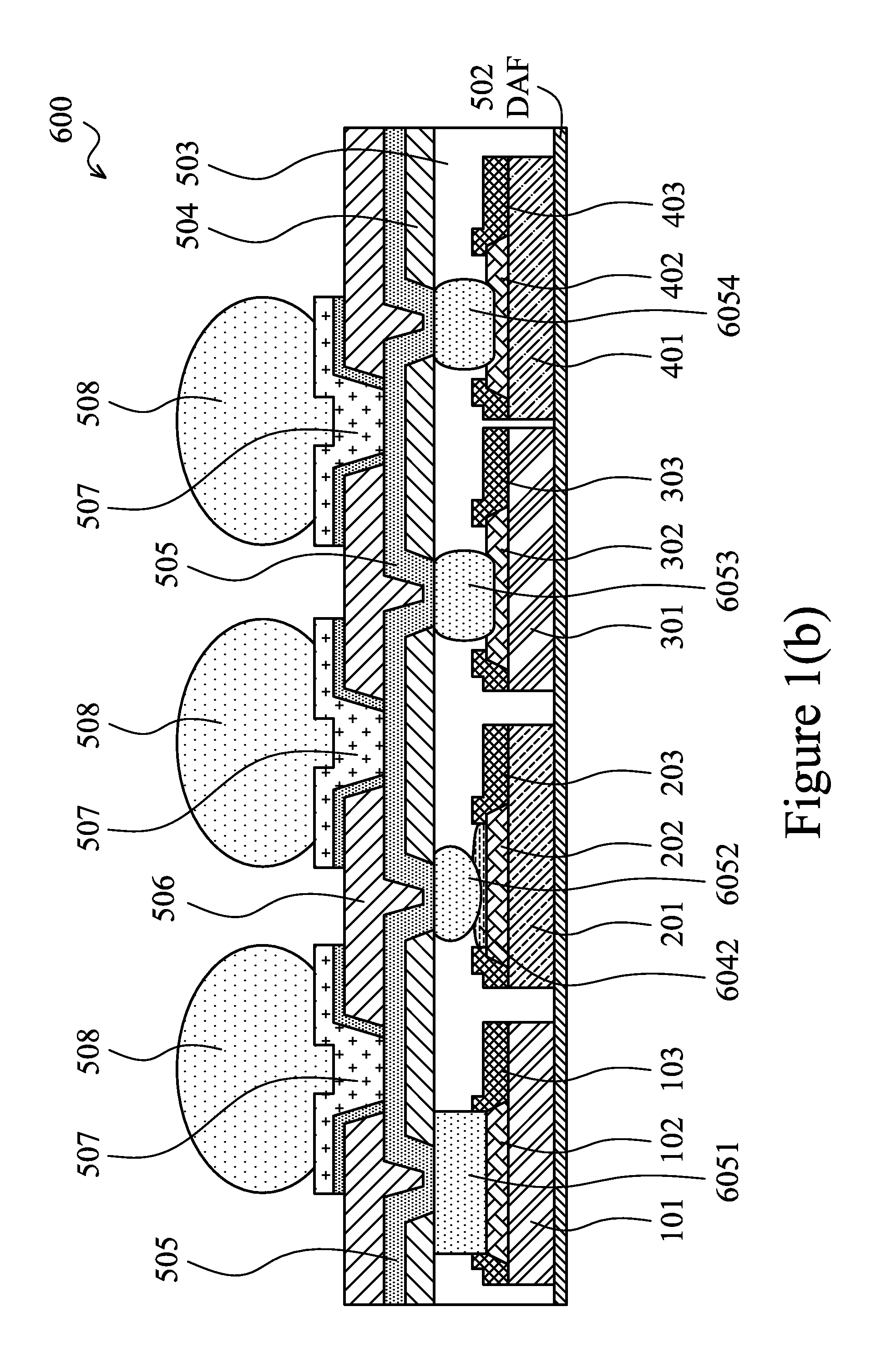
[0010]Wafer level packages (WLP) are commonly used for integrated circuits (ICs) demanding high speed, high density, and greater pin count. A WLP style semiconductor device involves mounting an active area of a die toward a chip carrier substrate or a printed circuit board (PCB). The electrical and mechanical interconnect is achieved through a plurality of connection devices, or simply called connections, such as conductive solder bumps or balls. The solder bumps are formed on bump pads or interconnect points or contact pads, which are disposed on the active ...


PUM


Abstract

Methods and apparatus are disclosed to form a WLP device that comprises a first chip made of a first technology, and a second chip made of a second technology different from the first technology packaged together by a molding material encapsulating the first chip and the second chip. A post passivation interconnect (PPI) line may be formed on the molding material connected to a first contact pad of the first chip by a first connection, and connected to a second contact pad of the second chip by a second connection, wherein the first connection and the second connection may be a Cu ball, a Cu via, a Cu stud, or other kinds of connections.

Description

BACKGROUND[0001]Semiconductor devices are used in a variety of electronic applications, such as personal computers, cell phones, digital cameras, and other electronic equipments. The semiconductor industry continues to improve the integration density of various electronic components (e.g., transistors, diodes, resistors, capacitors, etc.) by continual reductions in minimum feature size, which allow more components to be integrated into a given area. These smaller electronic components also require smaller packages that utilize less area than packages of the past, in some applications.[0002]One type of smaller package for semiconductor devices that has been developed is the wafer level package (WLP). A wafer-level package of integrated circuits (ICs) made of heterogeneous technologies, which may be referred as a heterogeneous integration, reduces manufacturing cost, while providing high performance and high density. Initial applications of heterogeneous integration, also referred to ...

Claims


Application Information

Patent Timeline
IPC IPC(8): H01L23/48H01L21/60H01L21/56
CPCH01L23/3128H01L21/561H01L2924/1461H01L24/19H01L23/64H01L25/0655H01L25/16H01L25/18H01L25/50H01L2224/244H01L2224/24101H01L2224/2101H01L24/05H01L24/13H01L24/20H01L24/24H01L21/6835H01L24/82H01L2221/68327H01L2224/0401H01L2224/04105H01L2224/05147H01L2224/05655H01L2224/12105H01L2224/131H01L2224/13147H01L2224/24011H01L2224/245H01L2224/82005H01L2224/82101H01L2224/05572H01L2224/24137H01L23/49816H01L23/49894H01L23/5389H01L2224/73267H01L21/568H01L2924/1305H01L2924/00014H01L2924/014H01L2924/00012H01L2924/01029H01L2924/01028H01L2924/01047H01L2924/01024H01L2924/01079H01L2924/01011H01L2924/00H01L2224/05552H01L2924/181H01L2224/94H01L2224/03
Inventor YU, CHEN-HUAYEH, DER-CHYANG
Owner TAIWAN SEMICON MFG CO LTD
Why Eureka
Try Eureka