Eureka AIR delivers breakthrough ideas for toughest innovation challenges, trusted by R&D personnel around the world.

Software and method for via spacing in a semiconductor device

Inactive Publication Date: 2013-10-24
GLOBALFOUNDRIES US INC
View PDF6 Cites 11 Cited by
  • Summary
  • Abstract
  • Description
  • Claims
  • Application Information

AI Technical Summary

Benefits of technology

This patent describes a method for determining the location of multiple power rail vias in a semiconductor device. The method involves assigning a location for each power rail via along the power rail, and ensuring that there is a minimum distance between the locations of the vias. It also includes determining any structures in the active region that may interfere with the power rail via, and changing the location of the power rail via to avoid interference. A computer-readable software product is provided to facilitate the execution of this method. The technical effect of this patent is to improve the accuracy and reliability of power rail placement in semiconductor devices, reducing interference and improving overall performance and reliability.

Problems solved by technology

However, the use of such a via pitch increases the resistance between the power rail and the transistors, thus reducing the electric performance of the transistors.

Method used


Image

  • Software and method for via spacing in a semiconductor device
  • Software and method for via spacing in a semiconductor device
  • Software and method for via spacing in a semiconductor device

Examples


Embodiment Construction

[0014]The following detailed description of the invention is merely exemplary in nature and is not intended to limit the invention or the application and uses of the invention. Furthermore, there is no intention to be bound by any theory presented in the preceding background of the invention or the following detailed description of the invention.

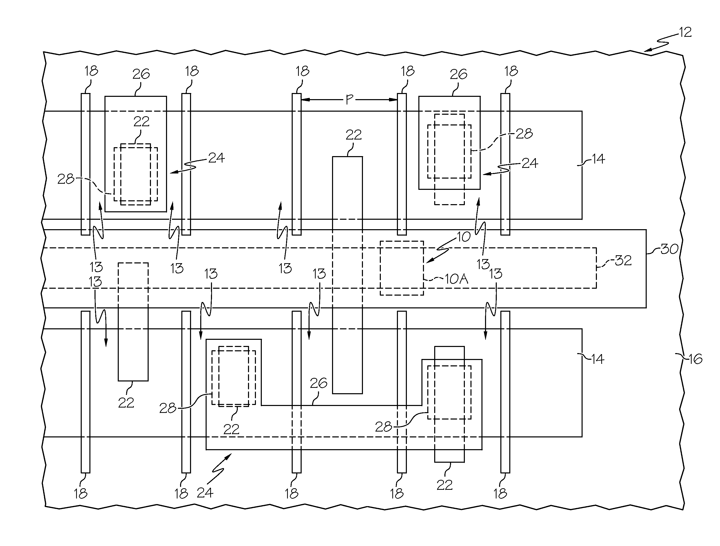
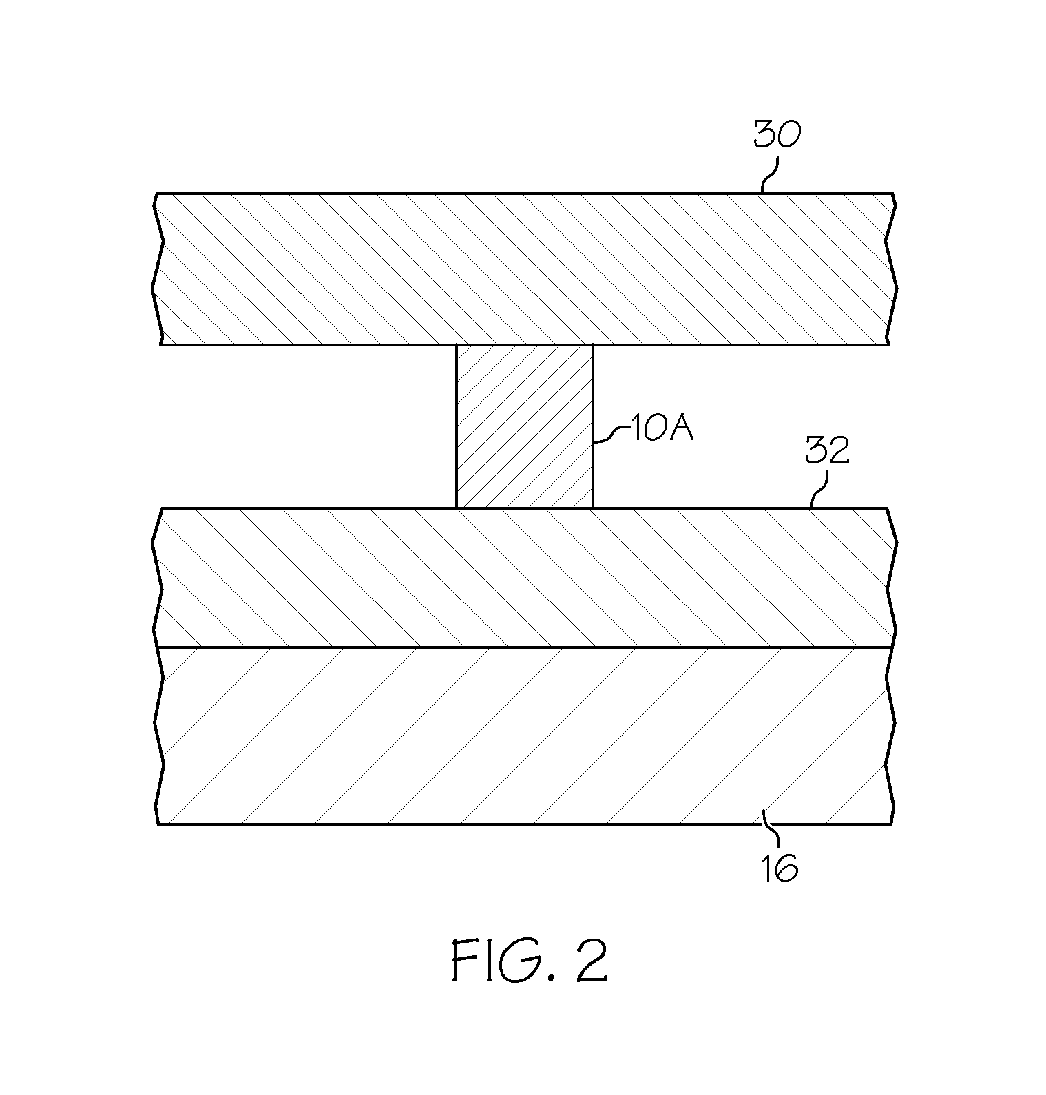
[0015]Referring to the figures, wherein like numerals indicate like parts throughout the several views, software and methods of determining the location of a plurality of power rail vias 10 in a semiconductor device 12 are shown and described herein. The semiconductor device 12 may be, for example, part of an integrated circuit, such as an application specific integrated circuit (“ASIC”) or a microprocessor. Of course, other embodiments, applications, and uses for the semiconductor device 12 described herein are recognized by those skilled in the art.

[0016]The semiconductor device 12 of the illustrated embodiment includes a plurality of tran...


PUM


Abstract

A computer-readable software product is provided for executing a method of determining the location of a plurality of power rail vias in a semiconductor device. The semiconductor device includes an active region and a power rail. Locations of a first via and a second via are assigned along the power rail. The spacing between the location of the first via and the location of the second via is a minimum spacing allowable. The spacing between the location of the second via and the locations of structures in the active region which may electrically interfere with the second via is determined. The location of the second via is changed in response to the spacing between the location of the second via and the location of one of the structures in the active region being less than a predetermined distance.

Description

FIELD OF THE INVENTION[0001]The present invention generally relates to semiconductor devices, and more particularly relates to power rail vias in semiconductor devices.BACKGROUND OF THE INVENTION[0002]Semiconductor devices having standard cell library logic (“standard cells”) often utilize a metal power rail to bring power and ground to the transistors forming the standard cells. In a common layout technique, standard cells are positioned above and below the power rail to maximize use of the power rail. A contact spine is typically disposed underneath and parallel to the power rail. A plurality of vias connects the metal rail to the contact spine. This contact spine is then electrically connected to contacts, which in turn, connect to the transistors.[0003]Typically, the pitch of the vias (i.e., the spacing between the vias) is larger than the pitch of the gates of the transistors. Most often, the via pitch is double that of the gate pitch. However, the use of such a via pitch incre...

Claims


Application Information

Patent Timeline
IPC IPC(8): H01L21/768G06F17/50
CPCH01L23/5286H01L2924/0002H01L2027/11881H01L27/0207H01L27/11807H01L2924/00
Inventor DOMAN, DAVID S.RASHED, MAHBUBTARRABIA, MARC
Owner GLOBALFOUNDRIES US INC
Why Eureka
Eureka Blog
Learn More