
Imaging Optical System, Imaging Device, and Digital Apparatus

a technology of optical system and imaging lens, applied in the field of imaging optical system, can solve the problems of difficult to shorten the total length of the imaging lens, difficult to correct comma aberration or chromatic aberration, and high error sensitivity

Active Publication Date: 2013-12-19
KONICA MINOLTA OPTICS
View PDF0 Cites 27 Cited by
  • Summary
  • Abstract
  • Description
  • Claims
  • Application Information

AI Technical Summary

Benefits of technology

The invention provides an imaging optical system that can correct various aberrations while being small in size. The system has a four-lens construction with specific refractive powers and positioning of the lens elements. The optical system satisfies certain conditions to achieve high quality imaging. The technical effects of the invention include improved image quality and reduced aberration correction. The imaging optical system can be applied to imaging devices and digital apparatuses.

Problems solved by technology

Accordingly, in the case where the user intends to obtain a wide angle of view with use of the imaging lens, it is difficult to correct comma aberration or chromatic aberration.
It is also difficult to shorten the total length of the imaging lens.
This may make error sensitivity extremely high, and may increase the performance variation at the time of assembling into an imaging lens.

Method used

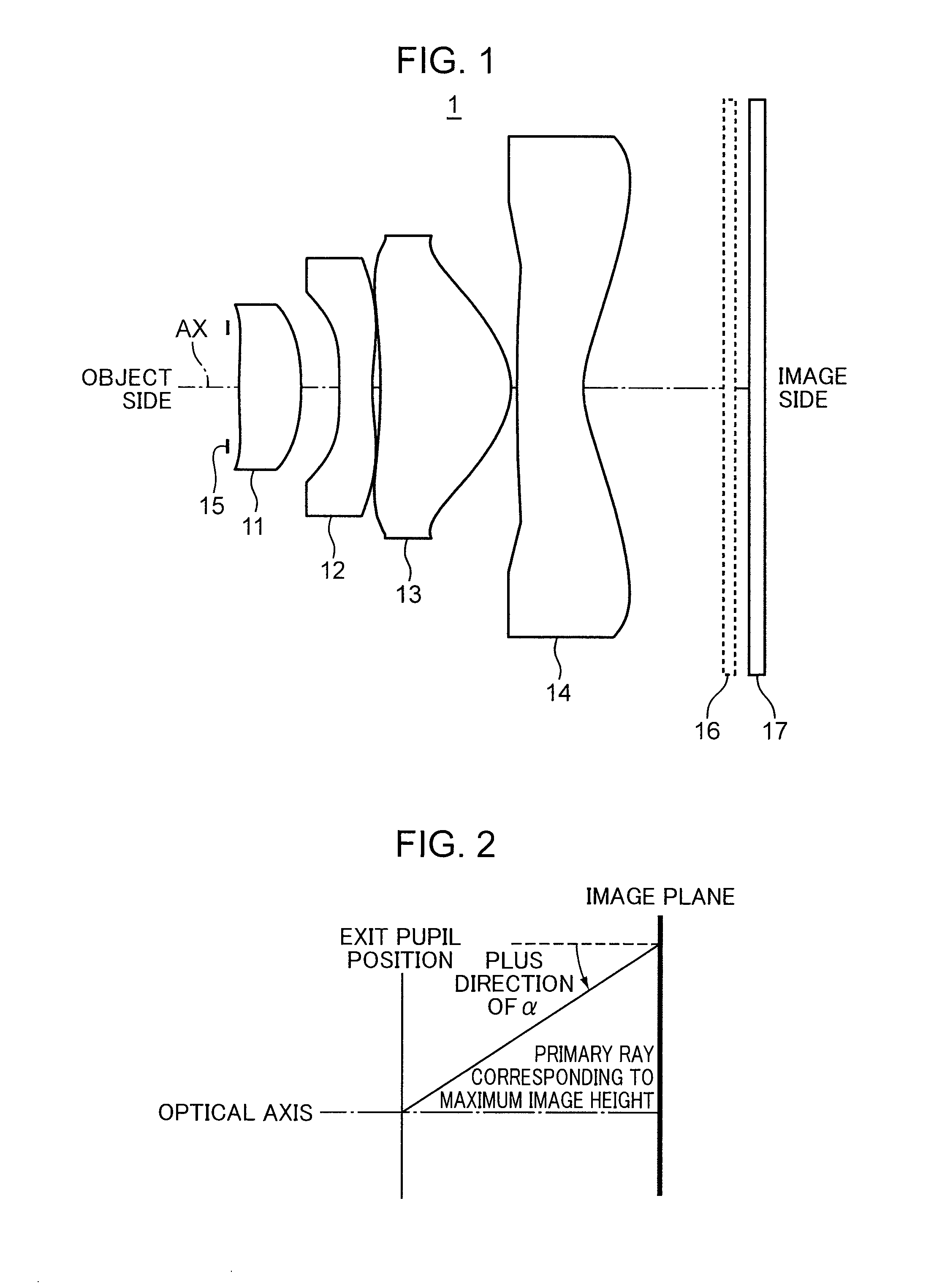

Image

  • Imaging Optical System, Imaging Device, and Digital Apparatus
  • Imaging Optical System, Imaging Device, and Digital Apparatus
  • Imaging Optical System, Imaging Device, and Digital Apparatus

Examples


examples

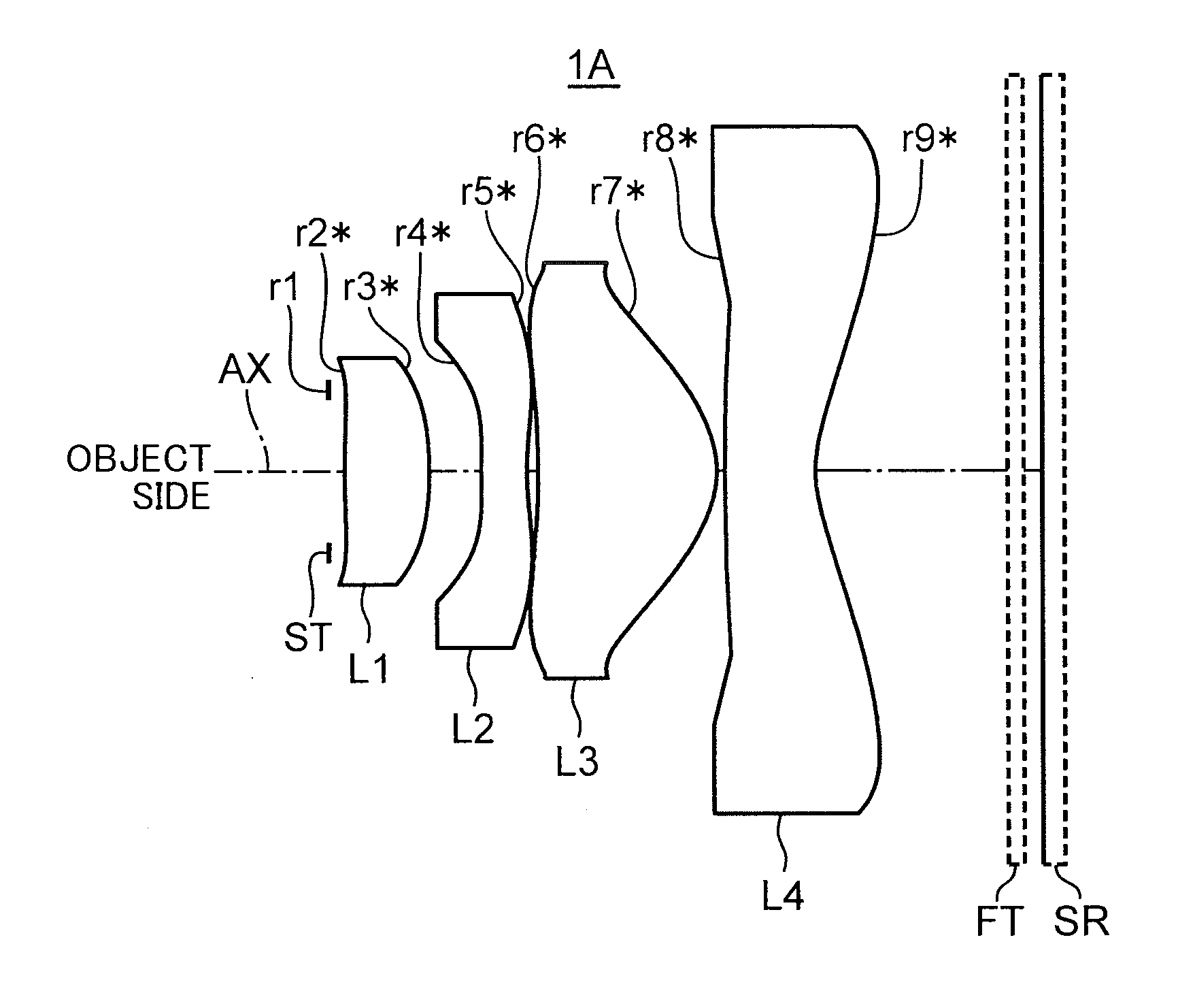
[0121]FIGS. 5 through 13 are sectional views showing arrangements of lens elements in imaging optical systems as Examples 1 through 9. FIGS. 14A through 22C are longitudinal aberration diagrams of the imaging optical systems as Examples 1 through 9.

[0122]As shown in FIGS. 5 through 13, each of the imaging optical systems 1A through 1I as Examples 1 through 9 is generally provided with a first lens element L1 having a positive refractive power, a second lens element L2 having a negative refractive power, a third lens element L3 having a positive refractive power, and a fourth lens element L4 having a negative refractive power. The first through fourth lens elements L1 through L4 are disposed in this order from the object side toward the image side. In performing a focusing operation, all the first through fourth lens elements L1 through L4 are integrally moved in the optical axis direction AX. Regarding the imaging optical systems 1A through 1I as Examples 1 through 9, the imaging op...


PUM


Abstract

An imaging optical system, an imaging device, and a digital apparatus have a four lens construction with positive, negative, positive, and negative refractive powers. A surface position at the maximum effective diameter of the second lens element is located on the object side than a surface vertex thereof. The fourth lens element has an inflection point at a position other than the intersection of the optical axis and the fourth lens element. The optical system satisfies the following conditions.0.7<f1 / f<5−0.8<(RS1+RS2) / (RS1−RS2)<3−3<(RS3+RS4) / (RS3−RS4)<20.03<d2 / TL<0.22W>72ν4>50,and0.55<Y / TL<0.8where f1 is a focal length of the first lens element, f is a focal length of the entire optical system, RS1, RS3, RS2, RS4 are curvature radii of the object-side surface and the image-side surface of the first and second lens elements, d2 is an optical axis distance between the first and second lens elements, TL is a total length of the entire optical system, W is a maximum half angle of view, ν4 is an Abbe number of the fourth lens element, and Y is a maximum image height.

Description

BACKGROUND OF THE INVENTION[0001]1. Field of the Invention[0002]The present invention relates to an imaging optical system, and more particularly to an imaging optical system suitably applied to a solid-state imaging element such as a CCD image sensor or a CMOS image sensor. The present invention further relates to an imaging device incorporated with the imaging optical system, and a digital apparatus loaded with the imaging device.[0003]2. Description of the Background Art[0004]In recent years, as high performance and miniaturization of an imaging element i.e. a solid-state imaging element such as a CCD (Charged Coupled Device) image sensor or a CMOS (Complementary Metal Oxide Semiconductor) image sensor have developed, digital apparatuses such as mobile phones or personal digital assistants incorporated with an imaging device using such an imaging element have been widely spread. There is also an increasing demand for miniaturization and high performance of an imaging optical syst...

Claims


Application Information

Patent Timeline
Patent Type & Authority Applications(United States)
IPC IPC(8): G02B3/00H04N5/232
CPCG02B3/00H04N5/23245G02B13/18G02B13/004G02B3/04H04N23/667
Inventor MATSUSAKA, KEIJITANAKA, HIROAKI
Owner KONICA MINOLTA OPTICS
Learn More