LCD device, manufacturing method and equipment for LCD panel

Active Publication Date: 2013-12-26
TCL CHINA STAR OPTOELECTRONICS TECH CO LTD
View PDF3 Cites 3 Cited by
  • Summary
  • Abstract
  • Description
  • Claims
  • Application Information

AI Technical Summary

Benefits of technology

[0035]The beneficial effects of the present invention are: the present invention has an electric conductive channel between the PVSA testing pad of the lower substrate and the transparent electrode of the upper substrate by using the first sealant such that the lower substrate and the

Problems solved by technology

However, it cannot avoid the action of the oblique light, and the influence of the making precision and positio

Method used


Image

  • LCD device, manufacturing method and equipment for LCD panel
  • LCD device, manufacturing method and equipment for LCD panel
  • LCD device, manufacturing method and equipment for LCD panel

Examples


Example

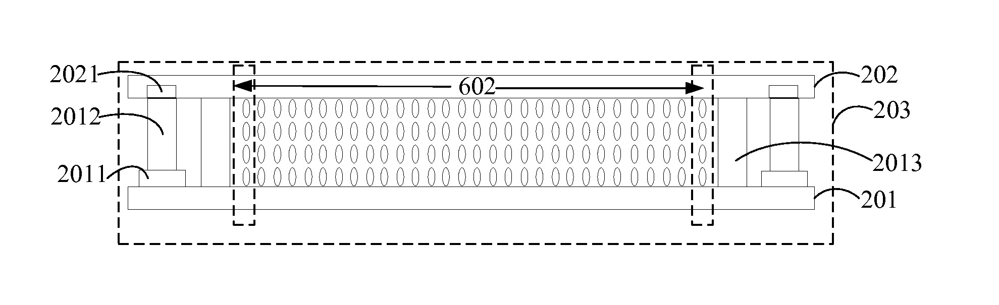
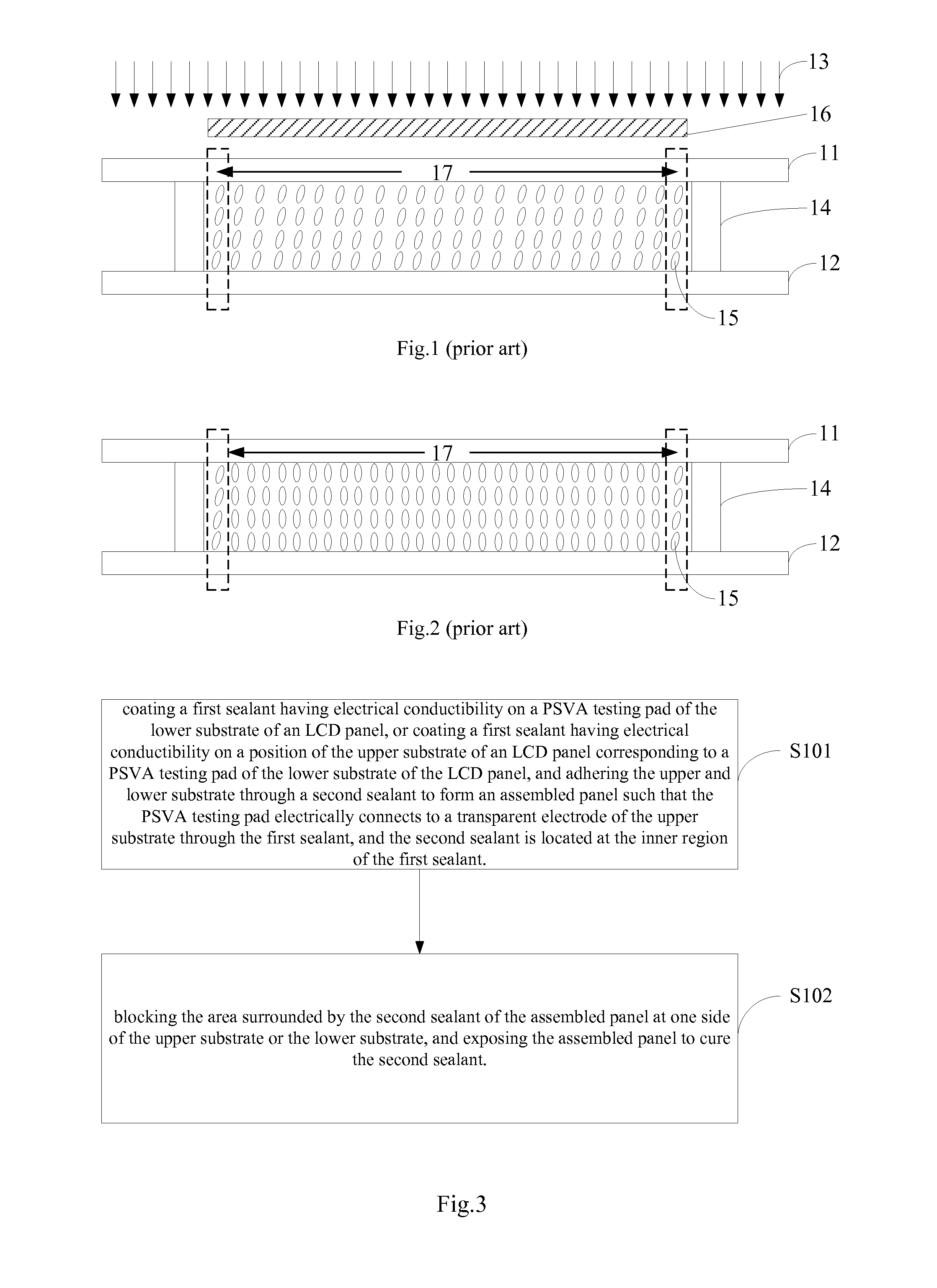
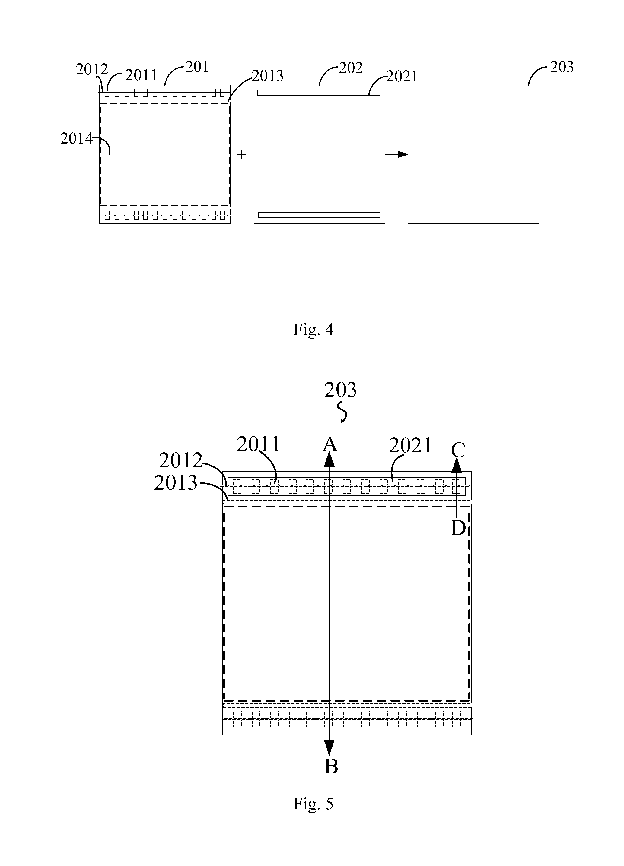
[0046]The manufacturing method for the LCD panel of the present invention can improve the uneven phenomenon around the screen of the active viewing area of LCD panel and to reduce the occurrence of broken bright spot and to be easier to realize narrow frame design of the LCD panel.

[0047]The following combines drawings and embodiments for detail description of the present invention.

[0048]Please refer to FIG. 3, a flow chart of a manufacturing method for the LCD panel of the present invention, including the steps:

[0049]Step S101: coating a first sealant having electrical conductibility on a PSVA testing pad of the lower substrate of an LCD panel, or coating a first sealant having electrical conductibility on a position of the upper substrate of an LCD panel corresponding to a PSVA testing pad of the lower substrate of the LCD panel, and adhering the upper and lower substrate through a second sealant to form an assembled panel such that the PSVA testing pad electrically connects to a t...


PUM

PropertyMeasurementUnit
Forceaaaaaaaaaa

Abstract

The present invention provides a manufacturing method for LCD panel by coating the first sealant having electrical conductibility on the PSVA testing pad of the lower substrate or on the position of the upper substrate corresponding to the PSVA testing pad of the lower substrate such that the PSVA testing pad electrically connects to the transparent electrode through the first sealant.
The present invention also provides a manufacturing method for the LCD device and a manufacturing equipment for the LCD panel. By the above ways, the present invention can improve the uneven phenomenon around the screen of the active viewing area of LCD panel and reduce the occurrence of broken bright spot and realize narrow frame design of the LCD panel.

Description

BACKGROUND OF THE INVENTION[0001]1. Field of the Invention[0002]The present invention relates to the field of LCD technology. More particularly, relates to a liquid crystal display (LCD) device, manufacturing method and equipment for an LCD panel.[0003]2. Description of Related Art[0004]PSVA (Polymer Stabilization Vertical Alignment) wide viewing angle technology enables the LCD panel to have a good black state, faster response time, and transmittance advantages. The PSVA type LCD panel, comparing to traditional LCD panel display, better to give users a higher level of visual experience, has gradually become the mainstream of development direction of the LCD panel.[0005]In PSVA manufacturing process, PSVA type LCD panel usually mixes light-sensitive monomer (Monomer) with the liquid crystal molecules between the upper and lower substrates or with the alignment film (PI. Polyimide) such that the monomer molecules condenses to the surface of the alignment film by UV irradiation or hea...

Claims


Application Information

Patent Timeline
IPC IPC(8): B32B37/24
CPCB32B37/24B32B37/12B32B2037/1253B32B2310/0831B32B2457/202G02F1/1339Y10T156/10
Inventor CHEN, CHENG-HUNG
Owner TCL CHINA STAR OPTOELECTRONICS TECH CO LTD
Why Eureka
Try Eureka