Augmented optical waveguide for use in an optical touch sensitive device

a technology of optical waveguides and optical touch, which is applied in the direction of user-computer interaction input/output, instruments, electric digital data processing, etc., can solve the problems of inability or difficulty to handle multitouch events, not scaling well to larger screen sizes as in displays used with laptops or even desktop computers,

Active Publication Date: 2014-01-30
BEECHROCK LTD
View PDF1 Cites 89 Cited by
  • Summary
  • Abstract
  • Description
  • Claims
  • Application Information

AI Technical Summary

Problems solved by technology

However, many of these approaches currently suffer from drawbacks.
For example, some technologies may function well for small sized displays, as used in many modern mobile phones, but do not scale well to larger screen sizes as in displays used with laptop or even desktop computers.
Another drawback for some technologies is their inability or difficulty in handling multitouch events.
Another drawback is that technologies may not be able to meet increasing resolution demands.
Another drawback for some optical touch-sensitive devices is that light propagation in optical waveguides in such devices may be altered by attaching materials (e.g., a display) with unknown optical properties to the optical waveguides.
Any object with unknown optical properties, or optical properties incompatible with TIR, that is in contact with the optical waveguide will likely reduce the optical energy propagating in the waveguide.
This may make measurement of touch-induced transmission loss more difficult and lower touch sensing robustness, adversely affecting the touch sensing performance of such an optical touch-sensitive device.

Method used


Image

  • Augmented optical waveguide for use in an optical touch sensitive device
  • Augmented optical waveguide for use in an optical touch sensitive device
  • Augmented optical waveguide for use in an optical touch sensitive device

Examples


Embodiment Construction

I. Introduction

[0036]A. Device Overview

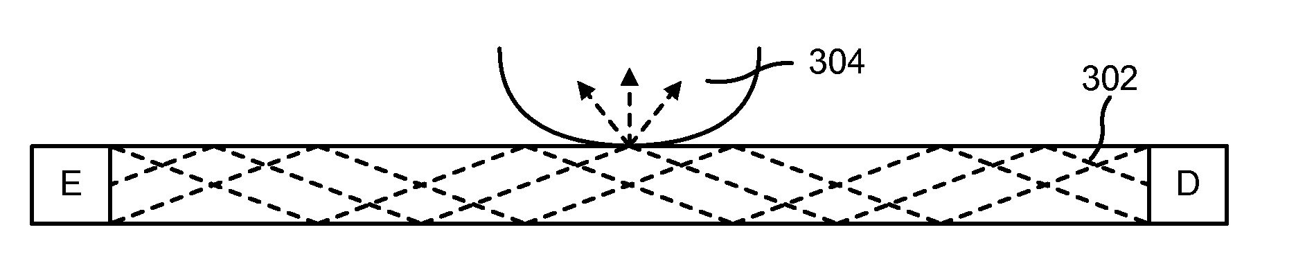
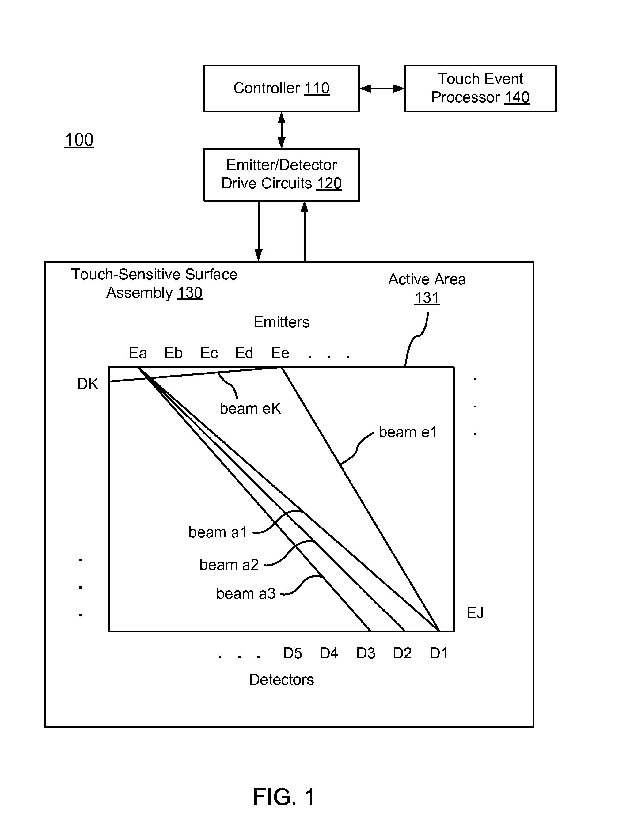
[0037]FIG. 1 is a diagram of an optical touch-sensitive device 100, according to one embodiment. The optical touch-sensitive device 100 includes a controller 110, emitter / detector drive circuits 120, and a touch-sensitive surface assembly 130. The surface assembly 130 includes an active area 131 over which touch events are to be detected. For convenience, the active area 131 may sometimes be referred to as the active surface or surface, as the active area itself may be an entirely passive structure such as an optical waveguide. The assembly 130 also includes emitters and detectors arranged along the periphery of the active area 131. In this example, there are J emitters labeled as Ea-EJ and K detectors labeled as D1-DK. The device also includes a touch event processor 140, which may be implemented as part of the controller 110 or separately as shown in FIG. 1. A standardized API may be used to communicate with the touch event processor 140, for...


PUM


Abstract

An optical touch-sensitive device is able to determine the locations of multiple simultaneous touch events. The optical touch-sensitive device includes multiple emitters and detectors coupled with an optical coupler assembly through a waveguide on the surface on the optical-touch sensitive device. Each emitter produces optical beams which propagate in the waveguide via total internal reflection and are received by the detectors. Touch events disturb the optical beams, and are determined based on the disturbances. The optical touch-sensitive device further includes an intermediate layer interposed between the waveguide and a display surface. The intermediate layer preserves optical beam propagation in the waveguide and is transparent to visible light. The optical touch-sensitive device may further include at least one frame zone, at least one dead zone, and/or at least one fixed graphics zone.

Description

CROSS REFERENCE To RELATED APPLICATIONS[0001]This application claims the benefit of U.S. Provisional Application No. 61 / 674,958, filed on Jul. 24, 2012, and U.S. Provisional Application No. 61 / 701,141, filed on Sep. 14, 2012, which are hereby incorporated by reference in their entirety.BACKGROUND[0002]1. Field of Art[0003]This invention generally relates to optical touch-sensitive devices, especially an augmented optical waveguide for use in an optical touch-sensitive device.[0004]2. Description of the Related Art[0005]Touch-sensitive displays for interacting with computing devices are becoming more common. A number of different technologies exist for implementing touch-sensitive displays and other touch-sensitive devices. Examples of these techniques include, for example, resistive touch screens, surface acoustic wave touch screens, capacitive touch screens and certain types of optical touch screens.[0006]However, many of these approaches currently suffer from drawbacks. For exampl...

Claims


Application Information

Patent Timeline
Patent Type & Authority Applications(United States)
IPC IPC(8): G06F3/03
CPCG06F3/0308G06F3/0421G02B6/10G06F2203/04103G06F2203/04107G06F2203/04109
Inventor DRUMM, OWENPIOT, JULIENCOPPERWHITE, ROBERT
Owner BEECHROCK LTD
Why Eureka
Try Eureka