
Reconstituted wafer-level package dram

a technology of reconstituted wafers and drams, applied in the field of microelectronic packages and assemblies, can solve problems such as complicated routing

Active Publication Date: 2014-02-06
INVENSAS CORP
View PDF27 Cites 11 Cited by
  • Summary
  • Abstract
  • Description
  • Claims
  • Application Information

AI Technical Summary

Benefits of technology

The present patent is about a microelectronic package that includes two encapsulated microelectronic elements. The elements are affixed together with their front or back surfaces facing each other. The encapsulants of the elements extend in at least one direction and make contact with the elements. The package also includes conductive interconnects that connect with the elements, and the interconnects can be exposed on the front or back surfaces of the elements. The technical effect of this design is that it allows for the efficient use of space and provides better performance and reliability in the microelectronic package.

Problems solved by technology

This can also lead to complicated routing and for different paths to externally-connected logic between chips of the same package.

Method used


Image

  • Reconstituted wafer-level package dram
  • Reconstituted wafer-level package dram
  • Reconstituted wafer-level package dram

Examples


Embodiment Construction

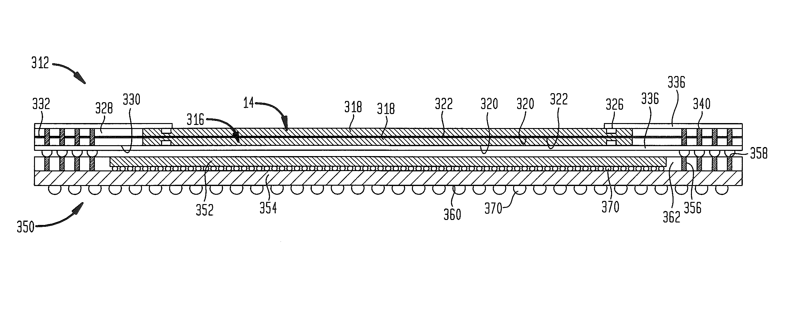
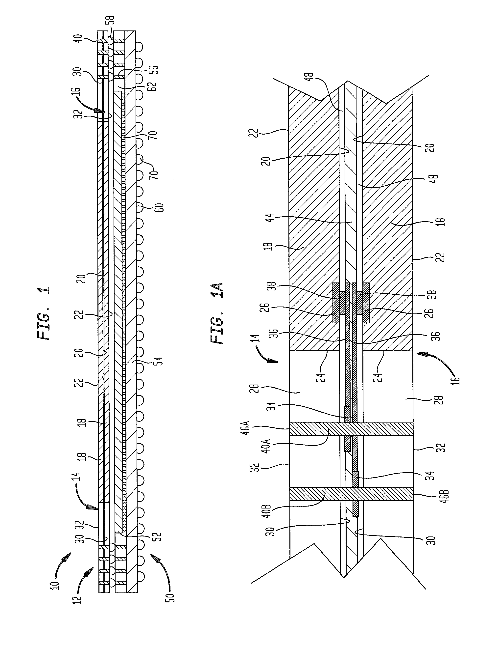
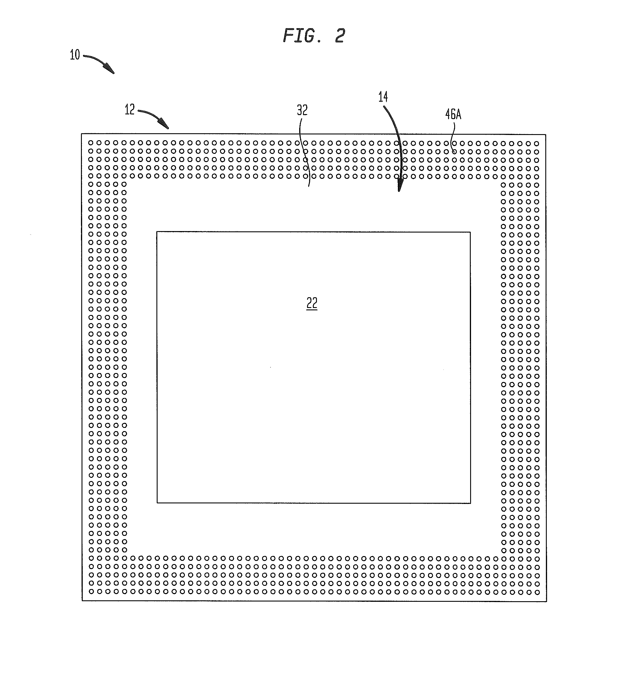
[0037]Turning now to the figures, where similar numeric references are used to indicate similar features, there is shown in FIG. 1 a microelectronic assembly 10 in the form a first microelectronic package 12 stacked over a second microelectronic package 50. In an example, assembly 10 can be in the form of a memory-on-logic assembly in which first package 12 is a memory package and second package 50 is a logic package, although the arrangements described herein can be used in arrangements with packages of different types or combinations of different types. Both first 12 and second 50 packages include one or more respective semiconductor dies 18 and 26 that themselves include a plurality of active devices. A memory package can be a package with semiconductor dies that have a majority of active devices configured for a memory storage array function. Similarly, a logic package can be one in which a majority of the active devices therein are configured to execute processor functions.

[003...


PUM


Abstract

A microelectronic package includes first and second encapsulated microelectronic elements, each of which includes a semiconductor die having a front face and contacts thereon. An encapsulant contacts at least an edge surface of each semiconductor die and extends in at least one lateral direction therefrom. Electrically conductive elements extend from the contacts and over the front face to locations overlying the encapsulant. The first and second microelectronic elements are affixed to one another such that one of the front or back surfaces of one of the first and second semiconductor dies is oriented towards one of the front or back surfaces of the other of the first and second semiconductor dies. A plurality of electrically conductive interconnects extend through the encapsulants of the first and second microelectronic elements and are electrically connected with at least one semiconductor die of the first and second microelectronic elements by the conductive elements.

Description

BACKGROUND OF THE INVENTION[0001]The subject matter of the present application relates to microelectronic packages and assemblies incorporating microelectronic packages.[0002]Semiconductor chips are commonly provided as individual, prepackaged units. A standard chip has a flat, rectangular body with a large front face having contacts connected to the internal circuitry of the chip. Each individual chip typically is contained in a package having external terminals which, in turn, are electrically connected to a circuit panel such as a printed circuit board and which connects the contacts of the chip to conductors of the circuit panel. In many conventional designs, the chip package occupies an area of the circuit panel considerably larger than the area of the chip itself. As used in this disclosure with reference to a flat chip having a front face, the “area of the chip” should be understood as referring to the area of the front face.[0003]Microelectronic packages may be fabricated at...

Claims


Application Information

Patent Timeline
Patent Type & Authority Applications(United States)
IPC IPC(8): H01L23/48H01L21/50
CPCH01L23/49811H01L2224/02381H01L25/105H01L25/18H01L2225/1023H01L2225/1058H01L2924/15311H01L2924/15321H01L2924/18161H01L2924/19107H01L2225/06558H01L2225/06565H01L2225/06548H01L25/0657H01L24/91H01L24/33H01L2924/12042H01L2224/16225H01L2224/0401H01L23/49838H01L2224/8203H01L2224/92144H01L2224/9202H01L2224/83855H01L2224/73259H01L2224/73253H01L2224/73217H01L2224/02379H01L2224/02371H01L2224/0233H01L2224/24147H01L2224/821H01L24/05H01L24/06H01L24/16H01L24/24H01L24/32H01L24/73H01L24/92H01L2224/04105H01L2224/06181H01L2224/12105H01L2224/16145H01L2224/16235H01L2224/24011H01L2224/2929H01L2224/293H01L2924/00014H05K3/4661H01L2924/00012H01L2924/00H01L2224/32145H01L2224/73267H01L2924/18162
Inventor MOHAMMED, ILYAS
Owner INVENSAS CORP
Learn More