Apparatus and method for inspecting pcb-mounted integrated circuits

a technology of integrated circuits and apparatus, applied in the direction of individual semiconductor device testing, contactless testing, instruments, etc., can solve the problems of inability to completely guarantee the soldering process, inability to test the integrity of the soldering process, and the formation of open contacts or short circuits

Active Publication Date: 2014-02-13
TWENTY TWENTY VISION
View PDF7 Cites 17 Cited by
  • Summary
  • Abstract
  • Description
  • Claims
  • Application Information

AI Technical Summary

Benefits of technology

[0036]According to another aspect of the invention for which protection is sought there is provided an apparatus adapted or arranged to perform a method as set out in any one or more of the preceding paragraphs in this Summary.

Problems solved by technology

On the other hand, as with many electronic systems, the soldering process is not wholly reliable and open contacts or short circuits maybe formed inadvertently.
In particular, since the solder balls are substantially non-compliant (that is, unable to flex), thermal or mechanical stresses caused, for example, by differences in coefficients of thermal expansion between the PCB substrate and the BGA package or by flexing and vibration of the PCB, may cause the solder joints to fracture.
In the case of BGA-mounted ICs, however, AOI systems are usually unable to measure the integrity of the solder joints due to the position of the connections on the underside of the IC package and are therefore generally limited to diagnosing missing components and placement errors.
This may lead to faults not being diagnosed using standard automated inspection techniques, resulting in faulty products and a loss of revenue for manufacturers.
If the measured drop is outside the predetermined range, the component is deemed to be mounted incorrectly.

Method used


Image

  • Apparatus and method for inspecting pcb-mounted integrated circuits
  • Apparatus and method for inspecting pcb-mounted integrated circuits
  • Apparatus and method for inspecting pcb-mounted integrated circuits

Examples


Embodiment Construction

[0045]The present invention will now be described, by way of example only, with reference to the accompanying drawings in which:

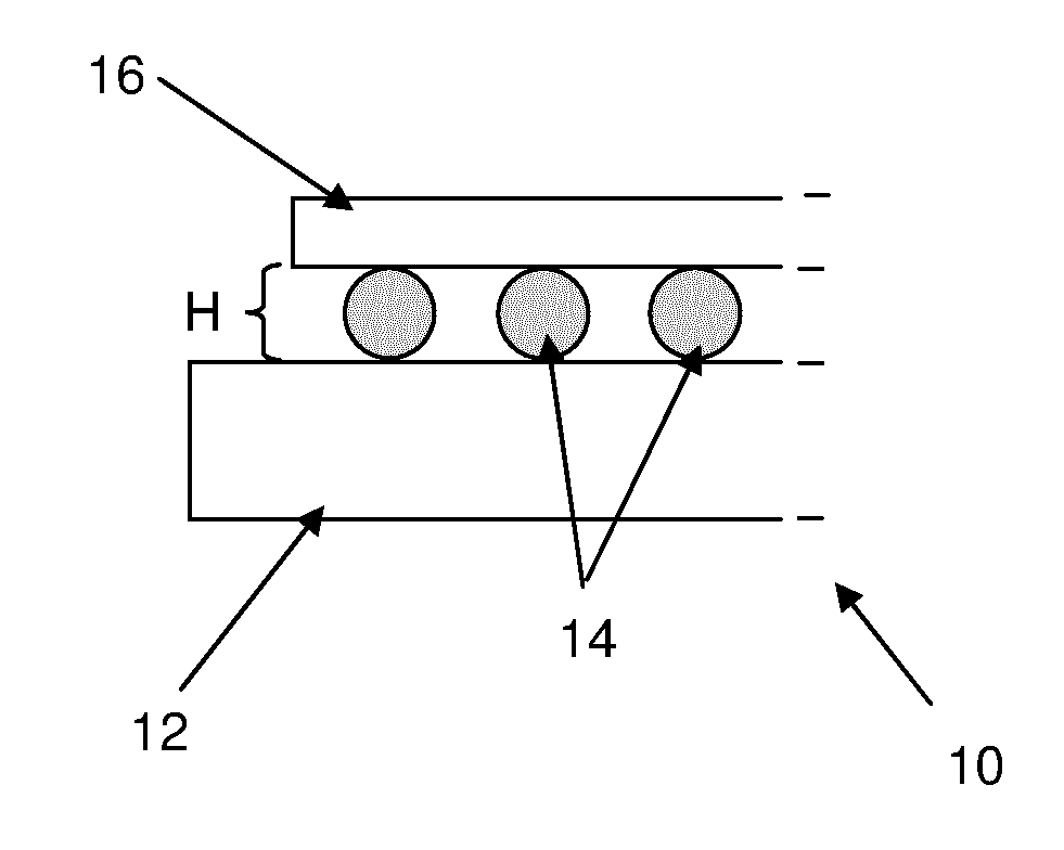
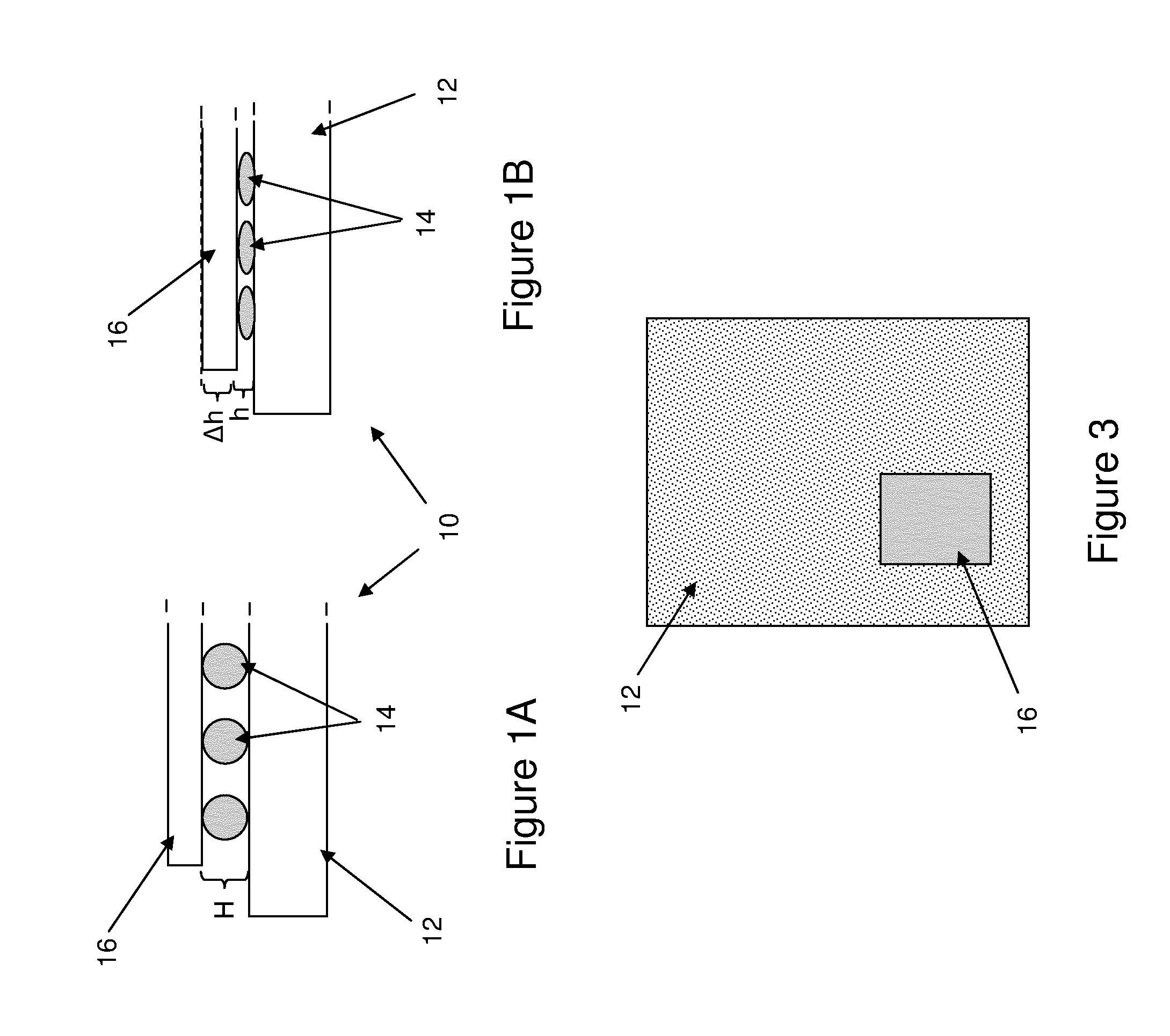
[0046]FIGS. 1A and 1B illustrate schematically sections through a solder joint between an IC and a PCB before and after soldering, respectively;

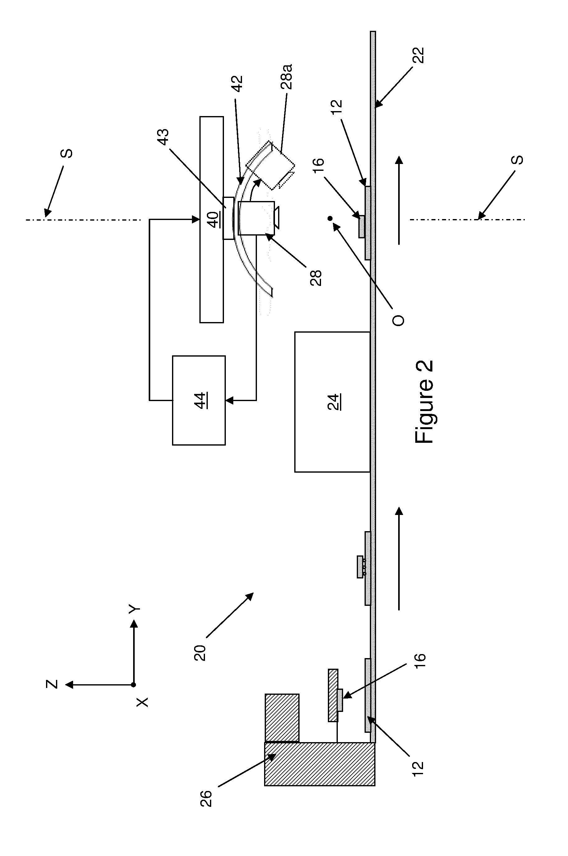
[0047]FIG. 2 illustrates schematically an apparatus embodying one form of the invention;

[0048]FIG. 3 is a plan schematic view of a PCB having an IC mounted thereon by means of a ball grid array;

[0049]FIG. 4 illustrates an example of a laser measurement device forming part of the apparatus of FIG. 2;

[0050]FIG. 5 illustrates operation of the laser measurement device of FIG. 4 in the apparatus of FIG. 2.

[0051]FIG. 6 shows an example of a first output trace from the laser measurement device; and

[0052]FIG. 7 illustrates an example of a second output trace from the laser measurement device.

[0053]Referring to FIG. 1A, which is schematic and not shown to scale, a portion of a BGA assembly prior to soldering is shown in cros...


PUM


Abstract

A method and apparatus for testing the mounting of an integrated circuit on a printed circuit board using a ball grid array comprises directing an inclined laser beam from a line scan laser sensor at the integrated circuit, detecting the position of the lower edge of the integrated circuit from laser light backscattered from the integrated circuit and printed circuit board, determining through a trigonometric calculation the height of the integrated circuit above the printed circuit board following soldering of the ball grid array and comparing the height with reference data. The integrated circuit is deemed to have been successfully mounted to the printed circuit board if the height falls within a predetermined range.

Description

INTRODUCTION [0001]The present invention relates to an apparatus and method for inspecting PCB-mounted integrated circuits and particularly, but not exclusively, integrated circuits mounted to a PCB or other substrate by means of a Ball Grid Array (BGA). Aspects of the invention relate to a method, to an apparatus, to an integrated circuit and to an electronic device.BACKGROUND TO THE INVENTION [0002]There are several techniques employed for surface-mounting integrated circuits (ICs) onto substrates such as printed circuit boards (PCBs). One common technique is the use of Ball Grid Arrays (BGAs) in which the pins of the IC are replaced by solder balls disposed on the underside of the IC package with the PCB carrying conductive pads in a pattern corresponding to the solder balls. In a technically-equivalent variation of this technique, the solder balls are formed instead on the PCB itself in a pattern that matches the pins of the IC.[0003]Mounting the IC package to the PCB involves p...

Claims


Application Information

Patent Timeline
Patent Type & Authority Applications(United States)
IPC IPC(8): G01R31/265
CPCG01R31/2656G01N21/956H05K13/0817G01N2021/95638G01B11/0608
Inventor BUTTERS, SIMONHALL, DAVID
Owner TWENTY TWENTY VISION
Why Eureka
Try Eureka